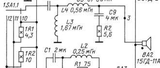
Schematic of Shushurin's 100 W tube ULF
The powerful 100 W UMZCH by V. Shushurin (MRB-1967) is designed to work with the equipment of an ensemble of electric musical instruments, and can also be used for sounding small halls and club rooms. This is a fairly powerful tube amplifier that provides an output power of about 100 watts.
Specifications
- The rated output power of the amplifier is 100 W.
- The harmonic coefficient at a frequency of 1000 Hz is no more than 0.8%, at frequencies of 30 and 18000 Hz - no more than 2%.
- In the frequency range 30-18000 Hz, the unevenness of the frequency response is +1 dB.
- Nominal sensitivity 500 mV, nominal output voltage at a load of 12.5 Ohms - 35 V.
- The amplifier noise level relative to the nominal output level is about -70 dB.
- Power consumption from the network is 380 VA.
Schematic diagram
The schematic diagram of the power amplifier is shown in the figure. The first two stages are made using lamps L1 and L2a. The second triode of a 6N6P (L2b) lamp is used in a phase-inverted stage with a divided load (R10 and R12).
The final stage of the amplifier is assembled according to a push-pull circuit using lamps LZ, Lb, and to provide the necessary power, two lamps are connected in parallel in each arm.
Rice. 1. Schematic diagram of a 100-watt low-frequency tube power amplifier.
To obtain a uniform frequency response and low nonlinear distortion, the last three stages of the amplifier are covered by deep negative voltage feedback. The feedback voltage is removed from the secondary winding of the output transformer Tr2 and is fed through the R19C8 chain to the cathode circuit of the lamp L2a.
Lamps L8-L6 of the final stage operate in AB mode. The negative bias to their control grids is supplied from a separate source - a half-wave rectifier on diode D7.
The anode circuits of the terminal lamps are powered by a full-wave rectifier using diodes D6-D13 connected in a bridge circuit, and the shielding grids of these lamps and the anode circuits of lamps L1 and L2 are powered by a rectifier using diodes D2-D5. Rectifier filters are capacitive. The capacitance of the filter capacitors is chosen such that when the power supplied by the amplifier changes from zero to the rated value, the supply voltage changes by no more than 10%.
Details and design
The power amplifier in the form of a separate, electrically and structurally complete unit is mounted on a metal chassis with dimensions 490X210X70 mm.
All vacuum tubes, transformers and electrolytic capacitors are installed on top of the chassis. The remaining parts are mounted in the chassis basement. The power transformer is made on a magnetic core LU32X80. window 32X80 mm.
Winding 1-2, designed for a mains voltage of 220 V, contains 374 turns of wire PEV-1 1.0, winding 5-4-85 turns of wire PEV-1 0.25, winding 5-6-790 turns of wire PEV-1 0 .55, winding 7-5-550 turns of wire PEV-1 0.41, winding 9-10-11 turns of wire PEV-1 0.9, windings L-12 and 13-14 - 11 turns of wire PEV-1 1 ,4.
Rice. 2. Arrangement of windings on the frame of the power transformer, diagram of the arrangement of winding sections on the frame.
The output transformer Tr2 is made on the same magnetic core as the power transformer. The windings are sectioned. Primary winding 1-3 consists of four sections of PEV-1 0.55 wire, 450 turns in each section.
The sections are connected in series, and a tap is made from the middle (pin 2). The secondary winding 4-5 consists of ten sections of PEV-1 0.55 wire connected in parallel, 130 turns in each section.
Provided that installation is correct, pre-tested parts are used and the output transformer is manufactured according to the recommended scheme, setting up a power amplifier comes down to setting the required bias voltage of the output stage lamps (-35 V) with a tuned resistor R41 and balancing the arms of the lamps of this stage with resistor R14.
It must be remembered that you cannot turn on the power amplifier without a load, as this can cause an electrical breakdown between the windings of the output transformer.
Shushurin. IN.
radiostorage.net
A. Kovalev
, Tyumen
Part one. Lyrics.
Recently, there has been a tendency to significantly increase the output power of audio amplifiers. 300 W is no longer the ultimate dream, and 100 W is considered insufficient to “squash and sausage.” And since the creation of amplifiers is driven by the requests of those who like to build something, there is a clear lack of high-quality developments in the power range from 20 to 50 W. Yes, you can object, they say, make a powerful amplifier, just don’t turn it on loudly, but this approach has one unpleasant property. It is called “noise and distortion level”. The fact is that amplifier noise is a fixed value for each implementation, as is distortion (more precisely, the proportion of distortion). And it is quite logical that the noise power at the output of a powerful amplifier is proportionally higher than that of a less powerful amplifier. By limiting the power with the volume control, we cannot in any way influence the noise level of the amplifier, but we influence the maximum amplitude of the output signal, which ultimately worsens the signal-to-noise ratio. About the same thing happens with the level of distortion. Distortion, of course, depends on the signal level, but most ULF implementations experience a relative increase in distortion as the signal level decreases below a certain threshold. Purely statistically, it is quite expected that the level of distortion of a powerful ULF with an output power of 1 W will be higher than that of, for example, a five-watt one (all other things being equal, of course). Why statistically? This is because the designs are different, and you can always find an example that runs counter to this statement, but in general the situation is like this.
Based on these considerations, the idea arose that it would be necessary to assemble something that could be used for home use - high-quality reproduction on household speakers of various stripes. This “something” must be traditional, i.e. from transistors and microcircuits, otherwise it would be possible to immediately take some kind of TDA, easy to configure and not have pitfalls in the form of sub-excitations, rejection of the capacitive component in the load, or, what is most unpleasant, through currents in the output stage.
Of course, I didn’t immediately rush to solder something, but to begin with, I was stuck in the simulator for a long time in order to “drive” popular amplifier circuits into it and see how they behave in these artificial conditions. After doing this, I came to the conclusion that, in general, all amplifiers are very similar. There are several basic variants of schemes (I won’t list them), and everything else is their improvements. This does not detract from the solutions used in newer and more advanced options, but that’s how it turned out.
| Module UNF-50-8 |
The schemes of Shushurin, Sukhov, Ageev, Solntsev and some others were modeled. Solutions from the Odyssey-010 and Radiotekhnika-101 amplifiers were also studied.
What did I understand for myself? The most important thing is to have only one voltage amplification stage. It will be very difficult to make two cascades, and even more so three, work in a common OOS loop, and a strong dependence on the connected load will appear. Second: it is desirable that the circuit be symmetrical for half-waves of the signal. The asymmetry, at best, will be limited to a rumble when turning the power on and off. At worst - an asymmetrical restriction, excitation of one shoulder when it is displaced, etc.... not very pleasant. You can add a third - avoid output stages with OE (and cascades with OE in general). Although in essence this is a continuation of the main thing. The problem here is that turning on a transistor with an OE has the worst frequency properties compared to other connections, and in the case when the transistor must also operate with a cutoff (output stage), another property appears: it turns out that the transistor does not like to turn off. Of course, textbooks drum this into us, but until you experience it yourself... In general, OE is out. ABOUT and OK are our everything.
By the way, we must pay tribute to the designers of the ULF-50-8 module, which was once used in the Radiotekhnika-101 amplifier, S70 speaker systems, and elsewhere. The module has very good parameters and, when transferred to a modern element base, has the right to a second life. But the end result of all this disgrace was the choice of Ageev’s amplifier as a prototype for further work - actual prototyping, testing, changes, etc. round. And perhaps we’ll return to ULF-50-8 later...
Part two. Scheme.
| Fig. 1 ULF circuit from the article “Amplifier block of an amateur audio complex”, A. Ageev, Radio magazine, 1982. No. 8, pp. 31-35 |
At its core, Ageev’s amplifier is a voltage amplifier stage made on an op-amp, followed by two current amplifier stages made on transistors, connected by emitter followers. The first stage of the current amplifier is loaded with resistors R7 and R9 (Fig. 1), which provide current to the bases of the output stage transistors. Moreover, such cross-connection of transistors gives two very valuable properties. The first is the exact repetition at the emitters of the output stage (V3, V4) of the voltage at the bases of the first (V1, V2). The second is excellent thermal compensation of the quiescent current, provided there is good thermal contact between all transistors.
The voltage amplifier also has a feature - a floating supply voltage. It is provided by connecting the midpoint of the op-amp power supply (R4, R5, V6, V7) to the amplifier output through resistor R6. This technique allows you to obtain from the op-amp an output voltage swing of up to 30 volts of amplitude, which makes it possible to ultimately have an output power of up to 60 watts.
The trouble with the original circuit is the low gain of the transistors. At low powers this is not critical, however, the simulation clearly showed that when operating at a 4 Ohm load as the power increases, the output transistors at the signal peaks clearly do not have enough base current. Of course, you can reduce R7 and R9, but this leads to an increase in the quiescent current and... there is still not enough current. It is for this reason that diode V5 and resistor R8 appeared in the original circuit (how they work is perfectly described in the original article).
As a result of searching for solutions to these problems, the following scheme was obtained.
| Fig.3 Area of safe operation of transistors of types BDX53 and BDX54 |
The basis of the scheme is exactly the same as in the distant 1980s. The voltage amplifier is made on DA1 type TL081 (domestic analogue of KR574UD4A), and the current amplifier is based on transistors: the first stage is VT7, VT8, and the second is VT9, VT11, VT13 and VT10, VT12, VT14 connected in parallel. The purpose of the remaining components is to ensure the functionality of these main components.
Probably the question immediately arises: “why are there so many parallel-connected transistors in the output stage?” In fact, this is a necessity. For semiconductors there is such a concept: “safe operating area” (OBR for short). OBR is the permissible combination of parameters of the current flowing through the transistor and the voltage drop across the transistor transitions. The key point is that even powerful transistors that allow multi-ampere K-E currents at a minimum voltage on this K-E, when the K-E voltage increases, cannot provide heat removal from the transition zone in the crystal, which is why the transistor overheats and fails. out of service. In order to avoid failures for this reason, the manufacturer declares the OBR for a specific type of transistor.
If the operating point of the transistor is within the OBR, the manufacturer guarantees that the transistor will not fail, degrade, or change in any other way. So that the transistors of the output stage are guaranteed not to leave the OBR when the amplifier is operating with a wide variety of loads, and they are installed in parallel.
| Fig.4 Internal structure of transistors of types BDX53 and BDX54 |
Those who have already estimated the modes of transistors when operating on a 4-ohm load may have already asked themselves, is the margin too big? The answer is straightforward - yes, the margin is more than sufficient even when the amplifier is operating on a load with a significant reactive component. But there is another reason for installing so many parallel transistors.
As already mentioned, the prototype lacks the transistor gain for normal operation of the output stage. Solving this problem is not difficult - we install Darlington transistors in the output stage rather than simple transistors (Fig. 4). Inside such a transistor there are, as we see, not one, but two transistors connected in a special way. But for the user “from the outside,” such a solution manifests itself as one transistor, only with a very high current gain (up to several thousand).
| Fig. 5 Dependence of the gain of transistors of types BDX53 and BDX54 on the current flowing through them |
This is very good and convenient, but there is one problem, which is shown in Fig. 5. It turns out that the gain of such a transistor depends significantly on the current flowing through it. The graphs clearly show that when the current changes from 0.1 A to 2.0 A, the gain increases by approximately 6.5 times, from ~700 to ~4500. But then, with a further increase in current, it begins to decrease again.
When the amplifier operates on a 4-ohm active load, with a power supply voltage of 24..28 volts, the maximum current in the load reaches 6-odd amperes. When installing three transistors in parallel, this current is divided equally between them (approximately, there is still a small spread due to the imperfection of their characteristics), and each gets 2 amperes of current. The result is a very favorable picture for us - as the current through the transistor increases, its gain also increases, which is why the required base current does not grow as quickly as it would if there were no such dependence. In this case, even under the worst conditions, the maximum base current of the transistor will not require more than 1 mA, i.e. 3 mA for all three - such a current with a reserve should be provided by the first stage of the emitter follower.
The first stage of the emitter follower is built on transistors of the same type, i.e. BDX53 and BDX54. This is done in order to obtain sufficient thermal stability of the amplifier without unnecessary problems. If you install other transistors, then they will have different (slightly, but this is quite enough) voltage drops at their junctions from those on the BDX53/54, which will cause difficulties both with setting the quiescent current and with its thermal compensation. This can be considered a disadvantage of such a scheme, but in my opinion this is not a great price to pay for stability of operation.
Instead of resistors R7, R9, which provide the base current of the output stage in the prototype circuit (Fig. 1), current generators are used here, made on transistors VT3, VT4 (Fig. 2) for the upper arm and, accordingly, VT5, VT6 for the lower arm . Resistors R11 and R14 set the value of this current. With a resistor resistance of 33 Ohms, the current is within 14..16 mA. It is noteworthy that VT4 and VT6 can be replaced with insulated gate field-effect transistors (MOSFETs) without significant modification of the circuit. You just need to add one zener diode to each transistor to protect its gate. This will allow the amplitude of the cascade output signal to increase by two to three hundred millivolts. But in reality this is a small gain, so in this design I decided not to do it.
The chain R15 and R16, installed in parallel with R14, is initially designed to provide adjustment of the lower-arm current generator within small limits in order to be able to set a current equal to the current in the upper arm. However, practice has shown that there is no need for this except for aesthetic reasons, so there is no need to install this chain. Just install resistors R11 and R14 of the same value (33 Ohms).
R12 and R13 compensate for the voltage drop from the flow of quiescent current through the equalizing resistors. Changing them also allows you to adjust the quiescent current. A decrease in resistance leads to a decrease in the quiescent current, an increase leads to an increase. The optimal range of these resistances is from 2.2 to 4.7 Ohms. With a resistance of 4.7 Ohms and a resistance of the equalizing resistors of 0.22 Ohms, the quiescent current is about 150..180 mA (50..60 mA for each output transistor).
Unfortunately, during actual operation, it happens that short circuits occur in the load, or extraneous voltages (currents) enter its circuit. To prevent failure of the output stage transistors in such cases, overcurrent protection is built into the output stage. It is implemented on transistors VT15.1 and VT15.2. If there is a short circuit in the load (or a significant decrease in its resistance), the increasing current through the output transistors leads to an increase in the voltage drop across the equalizing resistors R29, R30, R33, R34, R36, R37. When the voltage rises above a certain threshold, VT15 opens, which in turn switches the B-E transitions of the output transistors, thereby limiting the current in their bases, which does not allow the currents flowing into the load to grow indefinitely. VT15 itself is a transistor assembly, inside of which two separate transistors with an N-channel and a P-channel with fairly close parameters are located on one crystal.
Why was VT15 chosen as the field choice? I believe he is well suited for the job here. Figure 6 shows the curves obtained by simulating the mode with an excessively low load resistance. The upper graphs show the current through VT9 (the current through other transistors is similar), the lower graphs show the current through VT15. A sinusoid with an amplitude of 1.5 volts is supplied to the input of the amplifier. It is clearly seen that field-effect transistors have a clearer threshold at which they open. Having the same limiting threshold, the bipolar transistor VT15 already begins to influence the current of the output transistors, with its value being approximately 20% less than in the case when VT15 is field-effect. This means that when approaching the limiting threshold, distortion will be introduced into the amplified signal, the greater the closer the output stage is to the limiting threshold. The Field VT15 avoids this. The price you have to pay for this is a higher resistance of the equalizing resistors in the emitters of the output transistors.
| Fig.6 Features of the results of work on site VT15 field-effect and bipolar transistors. |
The voltage amplifier stage is made using op-amp DA1 type TL081. This is a widespread and fairly high-quality inexpensive op-amp. Its connection, similar to the prototype, is made according to a floating power supply circuit, which is provided by a divider on resistors R19, R20. The ratio of their resistances is chosen to ensure the necessary shift in supply voltages at the maximum amplitude of the output signal, but nothing more. Unfortunately, floating power will not allow such a connection scheme to increase the amplitude of the output signal as much as desired. This happens due to the fact that no matter how we shift the power supply, the potentials of the op-amp inputs still remain close to the potential of the common wire, and they must always remain within the potentials present on the op-amp power buses. This means that when shifting the op amp supply, the potentials of the power rails should not approach the potential of the common wire too close ( *
), not to mention changing the sign.
*
In truth, this is not always the case, because inclusion is possible to allow this, but it also has its limitations, which were unacceptable in this design.
To reduce uselessly dissipated heat on zener diodes and resistors, as well as to make it possible to choose a higher value of resistors R19, R20, the op-amp power supply is formed by parametric stabilizers made on transistors VT1 and VT2.
The input chain R1, R2, R3, R4 is connected so that it is possible to use both a balanced (symmetrical) connection of the amplifier input, and a conventional asymmetrical one. Balanced connection has the advantage of lower noise levels, especially noticeable when using long cords. To switch to an asymmetrical connection, it is enough to connect the “in-” input contact to the “Gnd” contact, but it is better to do this at the output of the signal source (pre-amplifier) than directly at the input of the power amplifier.
C1 and C2 reduce the level of ultrasonic components that can enter the amplifier input, and trimming resistor R6 allows you to balance the op-amp, thereby reducing the level of the DC component at the output of the amplifier.
The R9, C9 circuit is present to prevent the amplifier from being excited at high frequencies. Prototyping has shown that without this chain, excitation quite often occurs at frequencies from 9~10 MHz and an amplitude at the amplifier output from several tens to a hundred or two millivolts. This is accompanied by a significant increase in the quiescent current and, in some cases, subsequent failure of the output stage transistors.
R17 and R18, as well as R1, R3 and R5 form a chain of OOS signal dividers, which determines the gain. For the ratings indicated in the diagram, it is 20.5 dB (10.5 times) for asymmetrical connection and, accordingly, 41 dB (21 times) for symmetrical. Some change in the gain is possible - for this it is necessary to change the ratio of R17 and R18. However, you should not get carried away by a significant increase in the depth of feedback - this threatens the loss of stability of the amplifier,
The frequency response and phase response of the amplifier model with a closed feedback loop are presented in Figure 7, and the graphs of the loop gain and phase response of the feedback loop are shown in Figure 8.
| Fig. 7 Frequency response and phase response of the ULF model with a closed loop OOS. |
| Fig. 8 Frequency response and phase response of the OOS loop of the ULF model. |
Part three. Construction and details.
The design of the amplifier can be very diverse. There is no single form from which deviation would lead to problems. The only requirement that must be met is good thermal contact between the transistors of the emitter follower VT7-VT14. Therefore, it is advisable to place them on a single radiator and in a sufficiently crowded group so that there is no significant temperature difference between the transistors.
Transistors VT4 and VT6 dissipate up to half a watt of heat each, so they also need to be placed on radiators. This can be either a common radiator with the output stage, or a small individual one. Of course, according to manufacturers, a TO-220 case is capable of dissipating such power without a radiator, but in this case the temperature of the transistors can rise up to 60° above ambient temperature, which reduces the reliability of their operation, and significantly heated parts usually cause concern , especially for beginners.
As the basis of the design, a version of a printed circuit board measuring 135*60 mm was developed (Fig. 9). The board is double-sided, made in an industrial manner with metallization of the holes and the application of a solder mask.
All components except output transistors VT7-VT14 are mounted on the top side of the board.
| Fig.9 Top and bottom sides of the amplifier circuit board. |
Most SMD resistors are size 1206. Exceptions: resistors R19, R20 - because they dissipate relatively large power; resistor R39 - because a coil is wound on top of it, and resistors in the emitters of the output transistors - because significant current flows through them. The type of these resistors is BPR56 (Fig. 10)
The coil wound on top of resistor R39 contains 8-10 turns of copper winding wire with a diameter of 1.0 mm (Fig. 11)
Power supply and amplifier output connectors are 0.250″ (6.3mm) FASTON type terminals, widely used in automotive electronics. Such terminals are quite reliable, can withstand significant currents and are connected quickly enough, which is important when setting up or repairing.
Both vertical (Fig. 12) and horizontal (L-shaped) terminals can be installed. You can eliminate the terminals altogether by soldering the wires directly into the board, but this may be inconvenient.
| Fig. 10 Appearance of non-induction resistors type BPR56. | Fig. 11 Design of a coil placed on top of R39. | Fig.12 FASTON terminal. | Fig. 13 Collet socket for microcircuits. |
| Drawing of the FASTON terminal. |
The operational amplifier DA1 is type TL081, but can be replaced with other similar op-amps with a unity gain frequency of about 3-5 MHz. A good replacement would be the OPA134 - this op-amp has lower distortion and a slightly larger maximum output voltage swing, which will have a beneficial effect on output power. However, if you install OPA134, then R6 should not be installed, because this op-amp has different balancing circuits from the TL081 balancing circuits. Practice has shown that in most cases there is no need to balance the amplifier - even under the worst circumstances, the DC component at the output did not exceed 40 mV, which is quite safe.
If you want to install a socket for an operational amplifier in order to be able to easily change it during setup, then I recommend using so-called “collet” sockets - they fix the terminals much more reliably, which has a beneficial effect on the reliability of the design. Contacts of conventional sockets quickly lose elasticity when replacing microcircuits, which is why contact loss often occurs.
It is desirable that capacitors C1 and C9 be film. On the other hand, the use of ceramic capacitors with NP0 dielectric did not show any noticeable deterioration in performance.
| Fig. 14 Recommended method of insulating and pressing transistors to the radiator. |
Transistors VT7-VT14 are installed on a common radiator of sufficient size. The board itself is mounted on it, on stands 6 or 8 mm high. In this case, the housings of these transistors are partially under the board (see board drawing in Fig. 9). However, their installation on the upper side is not excluded, if the design of the radiator allows it.
Instead of the BDX53 and BDX54 transistors indicated in the diagram, you can use BDX33 and BDX34 transistors with similar parameters. It is possible to use TIP131, TIP132 (instead of BDX53) and TIP135, TIP136 (instead of BDX54). By coincidence, the amplifier was designed just for these transistors, but reality makes its own adjustments - transistors of the 'TIP' series are considered obsolete and are not produced.
Since the commonly used rubber insulating pads have a noticeable thermal resistance, to ensure its minimum value between all transistors, I recommend installing insulating pads not under each transistor, but using the design shown in Fig. 14. The essence of such a “sandwich” is that the transistors are in contact with the radiator not through the gasket, but directly with the heat-conducting plate, which in turn transfers heat to the radiator through the gasket, but with a much larger area. Thus, the influence of the gasket on the thermal resistance between the transistor and the radiator is reduced by the number of times the area of the gasket is greater than the area of the transistors themselves. This is a fairly noticeable value.
On the other hand, if you use mica spacers, then such a design is irrational for them, since, firstly, the material itself conducts heat much more efficiently, and secondly, you still have to look for spacers of this size... In this case, it is more convenient to put individual spacers under each transistor .
Transistors VT4 and VT6 can also be replaced with other types, for example BD239 and BD240 (with indexes 'B' or 'C'). You can use the widely used KT814, KT815 (with the indices 'B' or 'G') or their imported analogues BD139 and BD140, but when installed in this board they will have to be rotated 180° due to the mirror pinout in relation to the transistors indicated on the diagram. You also need to remember that they must be isolated from their radiators. If you are developing your own version of the board, all this is easy to provide for.
It is advisable to select zener diodes ZD1 and ZD2 so that their stabilization voltages are fairly close and, preferably, in the range from 17.0 to 17.5 volts. This helps to obtain the maximum signal swing at the output of the op-amp.
There are no special requirements for the power supply. Simple power supplies consisting of a transformer, a bridge bipolar rectifier and filter capacitors with a total capacity of 10~15 thousand uF in each arm are well suited. The optimal voltage on the secondary windings of the transformer (variable) is 24~26 volts. Transformer power is 100~150 W for each channel, or 200~250 W if there is one transformer for both channels.
The use of stabilized power supplies is still preferable. Firstly, this is due to the facilitation of the operating mode of the amplifier's output transistors, and secondly, this allows the amplifier to obtain the maximum power of which it is capable at the output of the amplifier. The optimal value of the stabilized supply voltage is 25-28 volts in each arm, and the peak current that the stabilizer must provide is 10 amperes for each amplifier channel.
| Fig. 15 Appearance of the finished amplifier module. |
| Fig. 16 Location of components on the board. |
L I T E R A T U R A: 1. A. Ageev. “Amplifier block of an amateur audio complex” - Radio magazine, 1982. No. 8, pp. 31-35 2. A. Ageev. “Parallel amplifier in UMZCH” - Radio magazine, 1985. No. 8, pp. 26-29 3. A. Ageev. “UMZCH with low nonlinear distortions” - Radio magazine, 1987. No. 2, pp. 26-29
© AK Laboratory
You can discuss the design in these places:
RadioKot website forum: https://radiokot.ru/forum/