CIRCUIT DESIGN OF OUTPUT CASCADES OF POWER AMPLIFIERS
Output stages based on "twos"
As a signal source we will use an alternating current generator with a tunable output resistance (from 100 Ohms to 10.1 kOhms) in steps of 2 kOhms (Fig. 3). Thus, when testing VCs at the maximum output resistance of the generator (10.1 kOhm), we will to some extent bring the operating mode of the tested VCs closer to a circuit with an open feedback loop, and in another (100 Ohm) - to a circuit with a closed feedback loop.
The main types of composite bipolar transistors (BT) are shown in Fig. 4. Most often, a composite Darlington transistor (Fig. 4a) based on two transistors of the same conductivity (“two” Darlington) is used in VC; less often, a composite Szyklai transistor (Fig. 4b) of two transistors of different conductivity with a current negative feedback is used. and even more rarely - a composite Bryston transistor (Bryston, Fig. 4c). The "diamond" transistor, a type of Sziklai compound transistor, is shown in Fig. 4 g. Unlike the Sziklai transistor, in this transistor, thanks to the “current mirror,” the collector current of both transistors VT 2 and VT 3 is almost the same. Sometimes the Sziklai transistor is used with a transmission coefficient greater than 1 (Fig. 4e). In this case, K P =1+ R 2/ R 1. Similar circuits can be obtained using field-effect transistors (FETs).
1.1. Output stages based on "twos". “Dvoyka” is a push-pull output stage with transistors connected according to the Darlington, Sziklai circuit or their combination (quasi-complementary stage, Bryston, etc.). A typical push-pull output stage based on a “deuce” Darlington is shown in Fig. 5. If emitter resistors R3, R4 (Fig. 10) of input transistors VT 1, VT 2 are connected to opposite power buses, then these transistors will operate without current cutoff, i.e. e. in class A mode.
Let's see what pairing the output transistors will give for the two "Darlingt she" (Fig. 13).
In Fig. Figure 15 shows a VK circuit used in one of the professional and onal amplifiers.
The Siklai scheme is less popular in VK (Fig. 18). At the early stages of the development of circuit design for transistor UMZCHs, quasi-complementary output stages were popular, when the upper arm was performed according to the Darlington circuit, and the lower one according to the Szyklai circuit. However, in the original version, the input impedance of the VC arms is asymmetrical, which leads to additional distortion. A modified version of such a VC with a Baxandall diode, which uses the base-emitter junction of the VT 3 transistor, is shown in Fig. 20.
In addition to the “twos” considered, there is a modification of the Bryston VC, in which the input transistors control transistors of one conductivity with the emitter current, and the collector current controls transistors of a different conductivity (Fig. 22). A similar cascade can be implemented on field-effect transistors, for example, Lateral MOSFET (Fig. 24).
The hybrid output stage according to the Sziklai circuit with field-effect transistors as outputs is shown in Fig. 28. Let's consider the circuit of a parallel amplifier using field-effect transistors (Fig. 30).
As an effective way to increase and stabilize the input resistance of a “two”, it is proposed to use a buffer at its input, for example, an emitter follower with a current generator in the emitter circuit (Fig. 32).
Of the “twos” considered, the worst in terms of phase deviation and bandwidth was the Szyklai VK. Let's see what using a buffer can do for such a cascade. If instead of one buffer you use two on transistors of different conductivities connected in parallel (Fig. 35), then you can expect a further improvement in the parameters and an increase in the input resistance. Of all the considered two-stage circuits, the Szyklai circuit with field-effect transistors showed itself to be the best in terms of nonlinear distortions. Let's see what installing a parallel buffer at its input will give (Fig. 37).
The parameters of the studied output stages are summarized in Table. 1 .
Analysis of the table allows us to draw the following conclusions: - any VC from “twos” on the BT as a load of the UN is poorly suited for working in a high-fidelity UMZCH; — the characteristics of a VC with a DC at the output depend little on the resistance of the signal source; — a buffer stage at the input of any of the “twos” on the BT increases the input impedance, reduces the inductive component of the output, expands the bandwidth and makes the parameters independent of the output impedance of the signal source; — VK Siklai with a DC at the output and a parallel buffer at the input (Fig. 37) has the highest characteristics (minimum distortion, maximum bandwidth, zero phase deviation in the audio range).
Output stages based on "triples"
In high-quality UMZCHs, three-stage structures are more often used: Darlington triplets, Shiklai with Darlington output transistors, Shiklai with Bryston output transistors and other combinations. One of the most popular output stages at present is a VC based on a composite Darlington transistor of three transistors (Fig. 39). In Fig. 41 shows a VC with cascade branching: the input repeaters simultaneously operate on two cascades, which, in turn, also operate on two cascades each, and the third stage is connected to a common output. As a result, quad transistors operate at the output of such a VC.
The VC circuit, in which composite Darlington transistors are used as output transistors, is shown in Fig. 43. The parameters of the VC in Fig. 43 can be significantly improved if you include at its input a parallel buffer cascade that has proven itself well with “twos” (Fig. 44).
Variant of VK Siklai according to the scheme in Fig. 4 g using composite Bryston transistors is shown in Fig. 46. In Fig. Figure 48 shows a version of the VC on Sziklai transistors (Fig. 4e) with a transmission coefficient of about 5, in which the input transistors operate in class A (thermostatization circuits are not shown).
In Fig. Figure 51 shows the VC according to the structure of the previous circuit only with a unit transmission coefficient. The review will be incomplete if we do not dwell on the output stage circuit with Hawksford nonlinearity correction shown in Fig. 53. Transistors VT 5 and VT 6 are composite Darlington transistors.
In order to eliminate the above-mentioned shortcomings of the circuit in Fig. 54 and simplify the circuit, we will replace the input emitter follower with a parallel follower, and resistors R 1 (Fig. 53) will be divided into 2 resistors (Fig. 55). At the connection points of the resistors (R 5, R 8 and R 6, R 9) we connect current generators (9 mA) on transistors VT 1, VT 4. and get the circuit shown in the figure.
Let's replace the output transistors with field-effect transistors of the Lateral type (Fig. 57
Anti-saturation circuits of output transistors contribute to increasing the reliability of amplifiers by eliminating through currents, which are especially dangerous when clipping high-frequency signals. Variants of such solutions are shown in Fig. 58. Through the upper diodes, excess base current is discharged into the collector of the transistor when approaching the saturation voltage. The saturation voltage of power transistors is usually in the range of 0.5...1.5 V, which approximately coincides with the voltage drop across the base-emitter junction. In the first option (Fig. 58a), due to the additional diode in the base circuit, the emitter-collector voltage does not reach the saturation voltage by about 0.6 V (voltage drop across the diode). The second circuit (Fig. 58b) requires the selection of resistors R 1 and R 2. The lower diodes in the circuits are designed to quickly turn off the transistors during pulse signals. Similar solutions are used in power switches.
Often, to improve the quality, UMZCHs are equipped with separate power supply, increased by 10...15 V for the input stage and voltage amplifier and decreased for the output stage. In this case, in order to avoid failure of the output transistors and reduce the overload of the pre-output transistors, it is necessary to use protective diodes. Let's consider this option using the example of modification of the circuit in Fig. 39. If the input voltage increases above the supply voltage of the output transistors, additional diodes VD 1, VD 2 open (Fig. 59), and the excess base current of transistors VT 1, VT 2 is dumped onto the power buses of the final transistors. In this case, the input voltage is not allowed to increase above the supply levels for the output stage of the VC and the collector current of transistors VT 1, VT 2 is reduced.
Bias circuits
Previously, for the purpose of simplification, instead of a bias circuit in the UMZCH, a separate voltage source was used. Many of the considered circuits, in particular, output stages with a parallel follower at the input, do not require bias circuits, which is their additional advantage. Now let's look at typical displacement circuits, which are shown in Fig. 60, 61.
Stable current generators. A number of standard circuits are widely used in modern UMZCHs: a differential cascade (DC), a current reflector (“current mirror”), a level shift circuit, a cascode (with serial and parallel power supply, the latter is also called a “broken cascode”), a stable generator current (GST), etc. Their correct use can significantly improve the technical characteristics of the UMZCH. We will estimate the parameters of the main GTS circuits (Fig. 62 - 6 6) using simulation. We will proceed from the fact that the GTS is a load of the UN and is connected in parallel with the VC. Let's study its properties using a technique similar to VC studies.
Current reflectors
The considered GTS circuits are a variant of a dynamic load for a single-cycle UN. In an UMZCH with one differential cascade (DC), to organize the counter dynamic load in the UN, they use the structure of a “current mirror” or, as it is also called, a “current reflector” (OT). This UMZCH structure was typical for the amplifiers of Holton, Hafler, and others. The main circuits of current reflectors are shown in Fig. 67. They can be either with a unity transmission coefficient (more precisely, close to 1), or with a greater or lesser unit (scale current reflectors). In the voltage amplifier, the OT current is in the range of 3...20 mA: Therefore, we will test all OTs at a current of, for example, about 10 mA according to the diagram in Fig. 68.
The test results are given in table. 3.
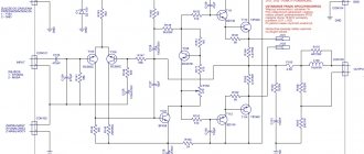
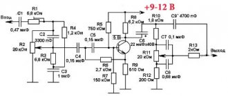
As an example of a real amplifier, the S. BOCK power amplifier circuit, published in the journal Radiomir, 201 1, No. 1, p. 5 - 7; No. 2, p. 5 - 7 Radiotechnika No. 11, 12/06
The author's goal was to build a power amplifier suitable for both sounding “space” during festive events and for discos. Of course, I wanted it to fit into a relatively small-sized body and be easily transported. Another requirement for it is the easy availability of components. In an effort to achieve Hi-Fi quality, I chose a complementary-symmetrical output stage circuit. The maximum output power of the amplifier was set at 300 W (into a 4 ohm load). With this power, the output voltage is approximately 35 V. Therefore, the UMZCH requires a bipolar supply voltage within 2×60 V. The amplifier circuit is shown in Fig. 1 . The UMZCH has an asymmetrical input. The input stage is formed by two differential amplifiers.
A. PETROV, Radiomir, 201 1, No. 4 - 12
Site administration address
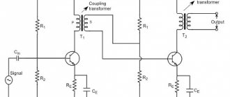
▍ Features of the operation of push-pull circuits
The use of push-pull circuits with AB operating mode provides a significant increase in output power while increasing efficiency.
Push-pull circuits have a lower nonlinear distortion coefficient compared to single-cycle ones due to better suppression of even-numbered harmonics. The quality of the output signal of push-pull circuits with AB operating mode is ensured by symmetry: the output stage lamps must be selected in pairs based on identical characteristics; halves of the primary winding must have identical amplitude-frequency and phase characteristics over the entire range of operating frequencies of the amplifier; the phase inverter stage must ensure phase shift accuracy throughout the entire amplitude-frequency range of the amplifier.
▍ Features of single-ended circuits
Single-ended circuits operate only in mode A and, compared to push-pull circuits using the same lamps, have lower output power and a lower efficiency.
The spectrum of the output signal of a single-ended circuit contains, among others, almost equal in level, the second and third harmonics. Single-ended circuits do not require selection of lamps. The design of a transformer for use in single-ended cascades is much simpler. Due to the operation of the lamp in mode A, the magnetic circuit of the output transformer is constantly biased, which significantly worsens its linearity.