Rebirth of Odysseus
Good afternoon, dear readers. Below the cut you will find a review of a homemade Class T power amplifier. For anyone interested in high-quality Chinese kits for amplifiers, please see below the cut. I have already introduced readers to my homemade amplifiers on Chinese kits (here and here), but now I wanted an amplifier that was more powerful and more functional for the future. The conditions were a power of about 100 W, several inputs, a remote control, a simple tone control.
Overview of components:
Amplifier board for TA 3020 Tripath
The price is in the title of the review.
Link to ebay Track and packaging
Reliable packaging:
The kit includes the board itself (without four capacitors in the power supply) and insulating spacers from Nomacon for 5 transistors: A fully equipped board is much more expensive. But still, the price tag for “digital” amplifiers is lower than for transistor ones of similar power.
Datasheet TA3020 As you can see, very good parameters are stated:
More about the TA3020 microcircuit The microcircuit is quite old, but is still sold, although the Tripath company no longer exists separately. Board dimensions: 185x115 mm - really healthy! Closer photo:
The quality of soldering and components is standard for Chinese boards.
Photo below
To operate, the amplifier requires two types of alternating voltage: dual 35-45 V up to 12 A and 12 V 1 A. Transistors irfp4227. There is a relay on the board to protect the speaker output. I installed power supply capacitors of 22000 uF 63 V.
Soft start board
Link to ebay Price 12$
Track and packaging
This board provides a smooth supply of mains voltage to the power transformer of the amplifier; this is important when using powerful transformers and large capacities in the power supply.
Nothing interesting below
Board dimensions: 90x60x25 mm, sold already soldered. The kit includes matching parts for the connectors. Switching up to 2 kW is declared, delay time is about 3 seconds.
Closer look at the power relay
Description of work
NTC thermistors (inrush current limiters) are usually included in the input circuits of power supplies, in series, to limit inrush currents. Their use in switching power supplies is driven by the desire to protect filter capacitors, rectifier diodes and other parts. When devices are connected to the network, the thermistor has a high resistance to the inrush current, which means that a large voltage “drops” across it, which causes a large current through the thermistor, the power released on the thermistor quickly heats it up and leads to a sharp drop in its resistance, a voltage drop across the thermistor tends to zero (but it will never be zero when the load is on, otherwise the thermistor will cool down and the “start” process will repeat - a kind of “generation” will appear), the thermistor, having limited the starting current, turns off.
The disadvantage is that there is a limit on the re-activation time, small, but there.
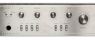
Digital volume control and input selector board
Link to ebay Price 37 $
Track and packaging
The packaging is reliable: a cardboard box, each board is wrapped in bubble wrap and covered with foam plastic.
What can this device do? — Input selector for 4 channels (you can connect, for example, a player, computer, TV, CD), 80 steps of volume adjustment, low and high frequency adjustment, balance adjustment, indication of all this is displayed on the display. For each input it remembers the settings. There is also a remote control and a multi-turn encoder that duplicate these functions. Plus, low distortion is claimed. By the way, by paying an extra $5 you can get an additional fee to turn on the amplifier from this remote control. Datasheet for the main chip LC75342
Adjustments
The device consists of two boards and an encoder and, of course, connecting wires.
Dimensions of the main board: 80x100x35 mm. Power required: 12-15 V DC or 10-15 V AC. There are also 4 pairs of input jacks and a signal output to the amplifier.
Display board dimensions: 48x120x34 mm. Visible display size: 14x64 mm. From board to display 24 mm. The display is two-line, the backlight is the favorite of the Chinese - bright blue. Remote control (by class=”aligncenter” width=”800″ height=”656″[/img] The buttons are all the same, which is not entirely ergonomic. There was no cr2025 battery.
Test run
passed successfully, along the way it also turned out that the device, when power is applied, is turned on only from the remote control. For those who are interested in this, but this device seems sophisticated, there is an alternative to Chinese kits with PGA2310. Not bad either, although not as functional.
Alternative
Refinement of the body:
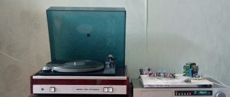
By chance, I received an Odyssey U-010 amplifier in a deplorable condition - instead of a power amplifier, it’s a knock-off from a TDA 7294, the body is scratched and rusty.
Was
Refinement of the front panel
There are a lot of holes in the front panel:
We seal them with epoxy cloth and putty on the front.
There is a lot of free space inside - what you need for a powerful amplifier.
The transformer was modified - poured half a liter of hot epoxy so that it would not hum.
Transformer
Secondary winding voltage 36 V - power approximately 250 W. And a low-current 8 V secondary. We paint with a primer from cylinders, install the fittings - this is what happens:
Modified body
The amplifier accessories, in addition to the connectors, include an electromagnetic interference mains filter, which is also a socket with a switch and fuse at the same time:
I bought it here aliexpress.com/item/10A-power-EMI-filter-CANNY-WELL-EMI-CW2B-10A-T/757701381.html $8.80 a year ago. The blue illuminated button is from here. We had to make an additional cover on the front panel of the amplifier in order to better place the screen:
Screen mount
The screen rests on a piece of plexiglass.
In general, a lot of mechanical work was done to refine the body. General assembly:
I sketched out a functional diagram:
In the diagram: 1. Electromagnetic interference filter. 2. Power transformer. 3. Additional transformer. 4. Smooth voltage supply board. 5. Illuminated power button. 6. Amplifier board. 7. Power capacitors. 8. Radiators. 9. Gain transistors. 10. TA3020 chip. 11. Input selector board. 12. Input selector screen. 13. Encoder for controlling volume and inputs. 14. Signal input. 15. Acoustic output.
As a result, about 130 W at 6 Ohms at 1% THD. THD at 50 W 0.03.
The sound is a little less detailed compared to the LM3886 amplifier, but with such power this is forgivable. And in terms of tonal balance, everything is even. Acoustics.
In the process of measuring and digging in the working amplifier, I burned the main TA3020 chip (((, ordered a new one, as soon as it arrives we will continue testing.
Thank you for your attention! All the best!
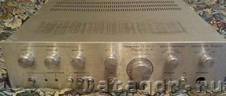
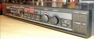
Improvement of the amplifier "Odyssey-U-010"
Once on the forum a question was asked: Which is better: “BRIG-U-001” or “Odyssey-U-010” ? I got into the discussion with my opinion that the Brig can be easily and quickly brought to mind, but with Odysseus you need to tinker, and even with an uncertain result. The opponents refused further discussion, considering my opinion unworthy of discussion.”
I wrote an article about Brig, which everyone still reads. And with opportunity, Odysseus came to me. There was an opportunity to compare. For two months I persistently dissected this miracle of Soviet technology made in Ukraine, determining the reasons for its indistinct sound. The results were disappointing:
- The structural diagram was chosen poorly. As a result, the noise of the preamplifier constantly sits in the speakers, regardless of the position of the volume control.
- The topology of the common wire is very ornate, and it is not possible to completely suppress the zzz sound in the speakers.
- Technical, installation and circuit solutions of UE and UM are stuffed with “highlights” of developers, the feasibility of which has not been confirmed by measurements and practice.
As a result, the modification of the amplifier turned out to be very “bloody”, therefore this material is not for the faint of heart, who are accustomed only to changing electrolytes and thickening the wires.
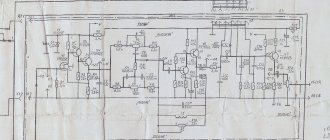
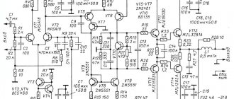
All changes to the scheme are reflected in this file [.djvu] on Google Drive. Deletions in the diagram are shown in blue, and newly introduced and changed elements are shown in red.
I will try to explain the reasons for the proposed changes.
Power supply A4 (BP)
Capacitors C3 and C4, mounted on a surface, are designed to suppress RF interference from the network. But at the same time they interfere with the transient processes of the diode bridge VD2-VD5, increasing the level of zzz reduction in the speakers in the absence of a signal. Since there are already C1 and C2 on the network, performing the same functions, it is quite possible to delete the indicated C3 and C4. Resistors R2-R5 are stoves designed to quickly discharge C5 and C6 when the power is turned off. Pure safety precautions. After carrying out all the work inside the case, before installing the casing, you can desolder them so as not to waste 5 W of transformer power. True, the network indication LED VD1 goes out for a very long time. If it’s annoying, you can reconnect it to the stabilizer output. Then we measure the output voltages of the powerful stabilizer and (if necessary) use resistors R23, R26 to set the initial ±37V. After all the modifications, I raised the output voltage of the stabilizer to ±40V and got an increase in pulse power, as well as cooler stabilizer radiators. But that's up to taste.
Pre-amplifier A3 (UP)
Input circuits. The rectangular signal supplied to the input of the UE, already at the input to DA1 and DA2, was enriched with surges of edges with an amplitude greater than the signal itself at small angles of rotation of the volume control (RG). As the angle of rotation of the RG increased, the amplitude of the emissions decreased. For a long time I could not understand the reason for this phenomenon. Finally it came to pass: the switching of C1 and C2 is carried out by section SA1.1 located on the UP board, and the complete signal from the source must run along the tracks of the printed circuit board back and forth. And next to them are signal paths from the RG engine with a much lower signal amplitude and high output impedance. As a result, we have the conditions for capacitive pickup from a conductor with a full signal to a parallel conductor from the RG engine. To get rid of this proximity, we had to abandon the switching of capacitors C1 and C2 and move them to the RG board, and ground the conductors to SA1.1 on the UP board. The emissions have almost disappeared. And after removing R4 and R7 they disappeared completely.
Loudness compensation. At the current level of audio technology, HF correction is not required, so R1, R2, C3 and C4 are immediately thrown into the trash. And the correction for low frequencies required some thought. GOST recommends making taps for loudness compensation at levels of 5-7% (lower) and 25-40% (upper) of the total resistance of the DG. If only one outlet is used, it is recommended to use the top one. In this case, one lower outlet is used, although there were all possibilities for connecting to the upper one. Moreover, capacitors C7 and C8 correspond to the upper tap, and resistors R5 and R6 correspond to the lower tap. I did not find a reasonable explanation for this confusion (other than ignorance of the subject). To somehow correct the situation, we had to increase the capacitance of C7 and C8 to 0.33 μF.
Cascade "Balance of frequency response". In general, a useless cascade. I would like to remove it, but the regulator on the front panel does not allow it. I had to comb it a little and keep it as harmless. I suspect that this cascade was the biggest “raisin” of the entire development, and perhaps even received a “Certificate of Authorship” for it. Analysis of the cascade circuitry showed that capacitors C21, C22, C27 and C28 do not separate anything and can be short-circuited, while capacitors C29 and C30 provoke surges at the fronts of the rectangular signal and can be removed.
"Tembroblock" cascade. This “miracle” of circuit design is annoying due to its unconventionality. While I figured out the RC circuits that determine the frequency response of the unit in the extreme positions of the regulators, I broke all my brains. But I found that capacitors C39, C45 (C40, C46) begin HF correction too early and it is advisable to reduce them to 0.047 μF, and to fully balance the bridge it is necessary to change R49 and R50 to 390 Ohms. Further analysis of the circuit design of this cascade showed that the current of the output repeaters (2x15 mA) on VT1-VT4 is unreasonably high, which leads to overheating of resistors R64 and R65 of the parametric stabilizers on VD5 and VD6. I had to increase R52 and R53 to 120 Ohms, and R64 and R65 to 820 Ohms. Further, capacitors C49 and C50 do not separate anything, and the cascade mode is well maintained by C37 and C38. Therefore, C49 and C50 can be short-circuited. Well, increasing C43 and C44 to 12 pF in the compensation circuit of the DA3 and DA4 microcircuits made it possible to slightly reduce their noise and increase stability.
Well, after several cosmetic operations, the preamplifier, so often reviled on audio forums, began to easily amplify and process the signal entering it, without enriching it with the products of its vital activity. And this despite the heavy structure and many suboptimal technical solutions. What is the value of the structure itself, bent in half with more than 50 wires and manually assembled regulators of all different ratings? This is a mockery of mass production and a complete disregard for maintainability. But this is not relevant to our business. Just the grumbling of a professional. Well, let's move on to new “miracles” of circuit design.
Power amplifier A5 (PA)
Typically, a PA is designed as an operational amplifier (op-amp) in a non-inverting connection, and an inverting connection is used when implementing a bridge circuit on two PAs. What made the developers go for the unconventional inverting connection of the PA? What are its advantages in these conditions? I didn’t find a clear answer right away. But when I discovered that the signal to the A1 overload board is removed from the base of the input transistor PA (VT1 or VT2), where its value is only a few microvolts, then desperately amplified thousands of times by cascades on VT6-VT8 and VT7-VT9 without feedback, it crept in suspicion of an emergency rescue of some difficult situation. After all, it’s hard to imagine a more unreasonable solution, since it was enough to move one resistor (R9 or R10) and get a normal signal level for the overload board. Suspicion began to grow stronger with further analysis of the adopted circuit solutions in the UM. It became clear that in pursuit of extremely low distortion figures, an additional amplifier stage was introduced on VT8 (VT11), which rotated the signal phase by 180º, which turned the traditional amplifier circuit into a generator. In order to preserve this stage, we had to change the amplifier circuit to inverting. And to ensure the stability of the resulting PA, it was covered with compensating capacitors (8 pieces per channel). In my opinion, this is overkill, and the decision made is wrong. As a result, it was decided to return the PA to a traditional non-inverting connection and clean the cascades from parasitic elements.
Transition to non-inverting switching:
- Input circuits. Remove C11, C12. We remove R11, R12 and solder them parallel to C5 and C6 from the print side. We short-circuit R9, R10.
- Feedback circuits. Remove C13, C14, R31, R32, C19, C20. We throw jumpers from resistors R48 and R49 to the bases of transistors VT9 and VT10, respectively. We replace C3 and C4 with non-polar 22 µF.
- Additional cascade. We remove VT8 and VT11, close the remaining contacts K-E. We cut off the connection of the VT9 collector with C52 and the VT10 collector with C53, respectively. We throw a jumper from the base of the remote VT8 to the base of VT15 and, accordingly, from the base of the remote VT11 to the base of VT20.
All. We rebuilt. The installation fits easily onto the printed circuit board. It is immediately necessary to reduce the gain in the VT6-VT8 and VT7-VT9 stages on the A1 overload board by removing electrolytes C8 and C9 and changing R32 to 82 kOhm, and R34 to 100 kOhm. Otherwise, when turned on, the overload will almost immediately light up and the output relay will switch off in an emergency.
Well, we have reached the level of the average serial amplifier of the 80s. I would recommend stopping here and listening to it for a week on your favorite acoustics in a quiet environment. For some, this level will be enough, because with the help of the “enhancement” knobs on the front panel you can get quite comfortable sound. But if you want to get comfortable sound with a linear frequency response (as is customary in Hi-End), then you need to go further. Which way to go is up to everyone to decide for themselves. I like my path. If you have your own path, then go, go and follow it. When you reach the intended point, pick up the keyboard and tell us about the key stages of the path traveled.
In the meantime, I will tell you about the stages of my journey to finalize this amplifier. So, let's begin.
Input stage. As in the ULF-50-8 amplifier “Radiotekhnika U-101” , to radically improve the sound quality it is necessary to change the operating mode of the transistor VT1 (VT2), for which we insert a resistor R121 (R122) of 18 kOhm into its collector. At the same time, the introduction of this resistor significantly increases the stability of the amplifier and makes it possible to remove almost all the compensating capacitors with which the PA is covered in its original form. In ULF-50-8, I managed to remove all the compensating capacitors in the OOS circuits, which baffled many experts, and my article was then called “illiterate.” But the criterion of truth is practice, and it has confirmed the correctness of the solution I proposed many times.
Rocking cascade. Consists of a cascode amplifier on VT15, VT16 (VT19, VT20) and a current source on VT17 (VT18). Everything would be fine. Has the right to exist. But at maximum amplitudes, emissions appeared again at the fronts of the rectangular signal. It turned out that in reality on the board instead of VD32+VD33+VD34 (VD39+VD40+VD41) there are resistors shunted with electrolytes, and instead of R115 (R116) there are VD7 (VD16) diodes. I dug further. In the current source, instead of VD35+VD36 (VD37+VD38), there is a current mirror on VT13 (VT14), again shunted by an electrolyte. This accumulation of electrolytes, coupled with the discrepancy between the print and the circuit, began to irritate me greatly, and I smashed this entire structure “to pieces and in half.” I restored resistors R115 (R116), but at a nominal value of 33 Ohms. I was going to replace VT15 (VT20) with KT502E, but my factory comrades got ahead of me. I threw out VT16 (VT19), and shorted the contacts K-E in print with a jumper. I removed the entire reference voltage circuit R34+VD32+VD33+VD34 (R37+VD39+VD40+VD41), or rather, everything that was there instead of what was drawn on the diagram. I removed the entire reference voltage circuit of the current source R35+VD35+VD36 (R36+VD37+VD38), or rather what was installed there, and powered the VT17 base from the VT5 base through a 200 Ohm resistor R123, and the VT18 base, respectively, from the VT6 base through a resistor R124. Well, the emissions are almost gone. They finally disappeared after removing all the compensating capacitors in the output stage.
Output stage. Usually this is a two or three-stage cascade with a common collector (CC), assembled according to a push-pull circuit. Here we have four stages with a phase reversal in the middle, and even with voltage gain. It was heavily involved, but not without benefit, as it turned out. The cascade has great thermal stability and does not require thermal contact of the initial bias circuit VD8-VD11 (VD12-VD15) with the heatsink for the output transistors, whereas for other circuit solutions of the output stage such contact is vital. This is good, of course, but why was it necessary to amplify the signal 13 times with transistor VT29 (VT30), then attenuate it with resistor R71 (R72), when it was enough to amplify the signal 3 times and transmit it entirely further? Further, why is the current through the first stage VT25-VT26 (VT27-VT28) 3 mA, and through the second stage VT29-VT30 (VT31-VT32) - only 1 mA? In my opinion it should be the other way around, i.e. the current should increase in steps. That's exactly what I did. Increased R53 (R54) to 2.7 kOhm, decreased R63, R66 (R67, R70) to 330 Ohm, shorted R71, R72 (R73, R74). Accordingly, I removed all the capacitors around these resistors C29-C32, C33, C34, C50, C51. Also removed C21, C22, C24, C27. But it was not possible to short-circuit R43, R51 (R52, R46) due to increasing distortion. I couldn’t find the reason yet, so I gave up. For stability margin, I increased C23 (C28) to 120 pF.
Setup. When turned on for the first time, a lack of no-load current (idle current) was detected by the voltage drop across R79, R80 (R81, R82). It was necessary to introduce additional D18 germanium diodes to the initial bias circuits VD8-VD11 (VD12-VD15). They probably lay in the trash for 50 years, waiting for their time. The XX current became normally regulated by resistor R39 (R42). I set it to 60 mV, which corresponds to a current of about 60 mA. It was also necessary to increase the PA gain, for which resistors R11, R12, R48, R49 were increased to 39 kOhm.
Well, that's almost all. During setup, it was discovered that the output relay K1 or K2 gets very hot, depending on the position of switch SA2. It turned out that the voltage to the relay winding is supplied with a smooth increase, so the winding is constantly under the starting current, which causes increased heating. It was necessary to organize a current surge, for which a D814A zener diode was installed instead of resistor R107, and resistor R6 with a resistance of 470 Ohms and a power of 1-2 W was inserted into the conductor supplying +37 V to switch SA2. As a result, the relay operates sharply, and a small current flows through it, and its body does not heat up.
And finally, about the connection of the common wire with the housing. Initially, two points of the housing are used: at the input connectors and at the point of connection of the front panel with the chassis, where the conductor from the common wire at the input to the PA is supplied. As a result, the left channel zzzs. An attempt to remove one of the body points leads to zzz-cutting in the right channel. I jumped, jumped around, danced with tambourines, nothing helps. So we had to embed a 1 Ohm resistor into the mentioned conductor from the common wire and thus reduce the quality factor of the ground loop. After this, the zzz-fishing interference smoothed out in both channels and became almost invisible. On this I calmed down.
Now it seems that's it. Maybe I missed something, so let my meticulous comrades fill it in. I won’t bore you with a description of measurements of output power, distortion, frequency response, etc. Everything is as usual. No miracles. You can collect and begin testing the strength of acoustics, walls, floors and the nerves of your neighbors. And since the sound of the amplifier has significantly cleared and softened, and has become comfortable with a linear frequency response, the listed tests can drag on for quite a long time.
Let's summarize. The sound quality of the amplifier has improved significantly. The sound is not tiring. I want to listen and listen. At the same time, I did not change the transistors to imported super analogues, did not touch the wires in the harnesses, did not change all the electrolytes to modern high-speed ones, did not change the connectors. I simply cleaned the cascades of debris, corrected the installation on the printed circuit board, and optimized unsuccessful circuit solutions. Along the way, I removed 12 electrolytes from the amplifier (I did not replace it, but threw it away as unnecessary), removed 6 transistors, threw out 20 ceramic and 4 film capacitors, removed 10 resistors, changed the values of 10 capacitors and 12 resistors, inserted 4 new resistors and 2 new diodes. Of course it turned out bloody, but what to do - too many unreasonable decisions ended up under the hood of this 10-kilogram monster.
This treatise was compiled on 04/26/2013
Author: Nikolay Vasilievich (Nivaga)
Modernization of amplifier Odyssey 010
Having read articles on the Internet like: replace the wires and sit, listen and enjoy, or here’s another gem worthy of attention “I recently replaced the KD203D power diodes in my Odyssey with Schottky 30CPQ100…. Damn, I didn’t expect such a difference. The LFs have simply transformed from uncertain, flopping lows; they have become collected, POWERFUL , so that you can feel them in your chest and the overload subjectively begins to blink much later than with Soviet diodes. Just class." The engineers simply racked their brains on how to reproduce low frequencies correctly, but it turns out that all you have to do is just change the diodes, get some beer and let it pound in your chest until it doesn’t. For example, I don’t understand where the lows will come from if you change the diodes, since after the diodes there are also 15,000 uF electrolytes, a stabilizer, and then only the ULF, which amplifies these very low frequencies, on which the number of low frequencies, as well as their quality.
Odyssey amplifier to me for modernization with a printout of what needs to be done.
1. Replace all electrolytes.
2.Change the output connectors for connecting the speakers.
3.Disable the buttons -10dB, -20dB, mono, reverse, LPF filter.
4.Replace the headphone jack with a jack.
5.Disable all input and recording selectors, leaving only one line input.
I turned on the amplifier to the network, checked it, of course there are no low frequencies, there are pulsations in the power supply, the amplifier lives its own life, it wants to work, it wants to be excited. There is no point in checking the parameters.
I removed all the electrolytes and checked them for functionality. Out of 30 capacitors, 9 were either dry or broken.
I replaced everything as agreed.
I just don’t see the point in changing the output connectors for connecting speakers, although not very beautiful, but made of copper, to fashionable ones made of audiophile iron, and it’s somehow impractical to buy at the price of an amplifier. In short, I dissuaded him.
Disabled unnecessary buttons.
Replaced the headphone jack.
I turned off all the input and recording selectors, and connected the linear input to the tone block board.
I turned on the amplifier, warmed it up for 20 minutes, set the ULF supply voltage to +- 37 V, the next adjustment of the ULF quiescent current in both channels was set to 20 mA.
I adjusted the voltage at the ULF output, in one channel 10mV in the other 20mV, the norm is 50mV.
I checked the output power up to the limit on a load of 8 ohms in one channel and got 23.8 V, in the other 23.5 V. Assigned 20 V on a load of 8 ohms is 50 W.
Adjusted the protection and ULF overload indicators.
I had to replace a couple of transistors because of which one ULF channel was excited.
That's all we can say. The amplifier has been slightly modernized, but rather tidied up and tuned.
The amplifier showed the main technical characteristics
| Nominal output power at 8 ohms | 50 W per channel |
| Maximum output power into 8 ohms | 70 and 69 W |
| Frequency range with unevenness + - 0.7 dB | 18-25000Hz |
| Harmonic distortion | 0,05% |
| Intermodulation distortion factor | 0,07% |
| Signal-to-noise ratio without filter (real) | 83dB |
Listening showed the amplifier sounds good but does not reach the highest class of sound. Firstly, despite the seemingly large number of high and low frequencies, they are not intelligible and are very loud when their level is added. The bass guitar and bass drum are difficult to distinguish, not to mention the double bass, which simply hummed on one note. Secondly, the high frequencies tsk-tsk-tsk and s-s-suck a lot. Many people love this sound and consider it to be of high quality.
Comparisons were carried out, so to speak, head-on, switching only amplifiers, on the 35AC I upgraded with the Radiotehnika U-101 , Odyssey U-010 and the CD Technics SL-PG 470A .
Measurements of the main technical parameters of the Odyssey U 010 amplifier
- < Back
Comments
-1 Pavel Rasskazov 07/26/2017 16:11 Thank you, but it looks like I’ve already figured it out, at least a little.
Quote
0 master 07/26/2017 11:57 My respect. Call the phone number on the website at the top of the page.
Quote
0 Pavel Rasskazov 05/29/2017 15:57 Can I contact you? I have the same amplifier1Do I have any questions about changing capacitors?????
Quote
-4 Alex 05/22/2014 18:42 Of the Soviet complete amplifiers, I liked the Brig-001, but not so much the Odyssey -010!
Quote
Update list of comments RSS feed of comments for this entry