Pulse Amplifier Design
The article discusses issues of designing pulse amplifiers on a modern element base without corrective inductances and approaches to their practical implementation.
Approaches to the design of pulse amplifiers differ from those typical for the design of harmonic signal amplifiers. When designing pulse amplifiers, it is necessary to know which or which of its parameters carry useful information. This could be: pulse duration (in this case, the bandwidth should be maximum), repetition rate or delay relative to a certain initial pulse. If low time delay is important, the amplifier's low-frequency bandwidth can be limited, reducing the effect of noise and interference. It is necessary to pay attention to the dynamic range of the amplifier, since it is the delay that depends on the amplitude of the signal that needs to be minimized. The delay, which does not depend on the amplitude of the input pulse, can simply be taken into account during further signal processing. This parameter becomes important if the amplifier is used as part of a measuring device, such as a rangefinder. It is easy to calculate that each nanosecond of delay is 0.165 m when measuring distance using the radar method. For sonar (the speed of ultrasonic wave propagation in water is approximately 1500 m/s), a delay of 1 μs is 0.75 mm of measurement accuracy. When designing, it is necessary to take into account the impedance (self-resistance) of the signal source. The question is not only in matching the signal source with the amplifier. The question is not to attenuate the signal at its input. For example, the dynamic resistance of the D608(A) detecting microwave diode lies in the range of 620 Ohms - 1.2 kOhms. If we connect a “standard” video amplifier with an input impedance of 50 Ohms to it, then the signal level at the amplifier input will be reduced by 28 dB. Can this be allowed when amplifying signals with an amplitude of several microvolts, if at the same time we need to amplify the pulse, for example, by 60 dB? Probably not - since in this case you will have to design the amplifier not at 60 dB, but at 88 dB, at a minimum. So we decided on the problem statement. Let's move on to practice.
The simplest amplifier
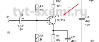
Let's start with the simplest device. For example, it is necessary to amplify a pulse signal of negative polarity with an amplitude of minus 20 mV to a level compatible with logic ICs, for example the 74HCxx series. That is, it is necessary not only to convert the polarity of the pulse, but also to amplify it to the value of its identification, as a logical unit. This level, according to the specification for the 74HCxx series IC, should not be lower than 4.2 V. That is, it is necessary to provide a gain of at least 46.5 dB or 210 times. For this example, it makes no sense to design the amplifier as a regular linear amplifier. It is enough to use a well-designed threshold device, simply a comparator or, if permissible, a Schmitt trigger. Considering the negative polarity of the input pulse and its relatively small value, the optimal circuit will be the one shown in Fig. 1 .
Rice. 1
The circuit is made on the comparator IC LM211 [1]. The unusual feature of the circuit is the approach to generating the reference voltage and the choice of output pulse polarity. The complexity of the divider to set the operating threshold is caused by the inevitable deviations in the values of the divider elements, the need for good filtering of the reference voltage, compensation of the input voltage offset voltage (for the LM211D it can reach 3 mV, and for the cheaper IC LM311D - 7.5 mV). In addition, it is impossible to guarantee that the supply voltage is exactly five volts. Thus, it is clear that it is impossible to do without adjusting the response threshold. A simple divider will not provide convenience and, most importantly, accuracy of adjustment for such low voltages as 20 mV. Therefore, the supply voltage is reduced by a divider to a level of approximately 150 mV, filtered and reduced to a voltage of 20 mV in the middle position of the rotor of the adjusted resistor R5 at a supply voltage of 5 V. The input resistance is set by choosing the value of resistor R4, and compensation for the difference in input currents is equal to the values of resistors R4 and R3. Now about the output signal of the comparator. Why was its inverse representation chosen? The answer is simple. The duration of the front of the output pulse in such a connection is much lower and practically does not depend on the installation capacitance and the input capacitance of the following circuits. Indeed, the discharge of these capacitors will be carried out through the open output transistor of the comparator. Otherwise, we would have them charged through the load resistance R2, which is much greater than the resistance of the open output transistor. According to the specification for the LM211D, this difference in the rise time for a 500 Ohm load is 4 times (25 not versus 100 not). It should be noted that good isolation along the power supply circuits (elements R1, C1, C2 and R9, C6) plays an important role for such devices. Otherwise, noise in the power supply circuits may disrupt its operation, especially when working with low levels of input signals.
Transistor amplifier
Now consider the following case. It is necessary to design a pulse amplifier from the detector head or sensor with an output impedance of 600 Ohms. Input voltage - pulses of positive polarity with an amplitude from 5 µV to 0.5 mV; the duration of a single pulse at level 0.5 is 500 ns; permissible delay time is no more than 200 ns. As in the previous case, the signal must be amplified to a level compatible with the 74HCxx series logic ICs. In this case, you must first amplify the signal to an acceptable level, and then use the circuit shown in Fig. 1. Thus, the gain of the preamplifier must be at least 20 mV/5 μV = 4000 times or 72 dB. What do manufacturing companies offer us? As was already shown at the beginning of the article, standard video amplifiers with an input impedance of 50 Ohms are not suitable for this purpose. Let's turn to integrated circuits. Indeed, such ICs exist. For example, AD810 [2]. The microcircuit has a delay time of no more than 50 ns, but the maximum permissible gain is 20 dB (10 times) and the bandwidth is 50 MHz
(with power supply ±5 V). The situation is similar with other ICs, most of which are used as repeaters or as amplifiers with a gain of 2 to 5. You can, of course, cascade such ICs, but they consume a current of about 8 mA and have a high price (5 USD or more).
The way out of the above situation is to build an amplifier using discrete elements. We will not consider in detail the typical circuits of such amplifiers. Typically this is a multi-stage amplifier, made according to a circuit with a common emitter, a base divider and sometimes a negative feedback circuit in the form of a resistor in the emitter circuit. The number of stages is determined by the parameters of the transistors and the gain. To increase the bandwidth, frequency correction is used in the form of capacitors in the emitter circuits and/or chokes in the collectors of transistors. An example of a link of such a typical “classical” amplifier is shown in Fig. 2.
Rice. 2
The methodology for their design has been described many times and in detail. There is no doubt that amplifiers with galvanic coupling are more convenient for use, but the technique for their projection is not so accessible. So where to start? First, we need to decide what impulse or impulses we will be dealing with. Secondly, what level of overload should we provide without disrupting the operation of the device. In our technical specifications (see above), these parameters are specified: a rectangular pulse of positive polarity, pulse duration t=500 ns, overload 40 dB. We determined the gain to be at least 72 dB. At the next stage, it is necessary to determine a parameter such as the amplifier bandwidth. We consider the “worst case” - a rectangular pulse (in reality the pulse will be in the shape of a trapezoid with exponential fronts) and single. From the theory of circuits and signals it is known that the narrower the pulse, the wider its spectrum. To reduce the delay time, it is necessary to provide a passband with a cutoff frequency close to 1/t. Thus, the upper operating frequency of the amplifier should be 1/500 ns = 2 MHz. At first glance, this condition is simple to fulfill and almost any transistors can be used. It turns out - no. Here it is necessary to take into account that the limiting frequency of current amplification of transistors fT (transition frequency) is really limiting and a transistor with fT = 400 MHz will not always provide sufficient amplification of signals requiring a frequency of fc = 2 MHz without taking special measures. The literature provides many recommendations for choosing transistors. But they are either very approximate or contain parameters that are not available in the specifications (for example, volumetric base resistance) or require full calculations of the amplifier followed by multiple approximations. To select transistors, you can use an empirical formula (please note, this formula is only an estimate), which was derived by the author of the article during his many years of engineering practice: fT>M*fc*hFE*K, where hFE is the maximum current gain ( DC current gain) in the selected mode; K is the desired cascade gain; M is a coefficient depending on the type of transistors.
For npn transistors it is 0.2-0.5 for pnp transistors - 1-3. And so, if we put K = 20 dB (10 times), either an npn transistor with fT>0.5*fc*100*10=1000 MHz, or a pnp transistor with fT>1*fc*100*10=2000 MHz is needed . In this case, we set hFE =100.
What do we get from such an analysis?
We find that when using transistors that meet these requirements, a transistor in an amplifier cascade with K = 20 dB can be considered as a transistor in which the base current vector does not have an additional shift at the upper amplification frequency we need. That is, it does not need high-frequency correction elements (inductor L1 and capacitor SZ in Fig. 2) and can be considered as a transistor operating in the low-frequency region, which simplifies calculations and the circuit as a whole. As transistors suitable for this criterion, we can suggest, for example, the BFS17A [3] and BFT92W [4] transistors. The first has fT = 2.8 GHz with a maximum hFE = 90, the second fT = 4 GHz with hFE = 50. For these transistors we can set the gain to K» 30 dB. The total gain is 72 dB, so it is enough to have 3 amplification stages or, with some deterioration in the parameters, 2.
Three-stage amplifier with galvanic coupling
Let's choose a three-stage amplifier. Since we are dealing with pulses of positive polarity, it is better to use the BFS17A transistor in the first stage, which will operate on opening and, as shown above, will provide a shorter delay time on the leading edge. After the phase reversal, we use BFT92W (the reason for this choice will be explained below), and then again BFS17A. As a base we use the diagram shown in Fig. 3 .
The circuit is a transistor triple with a bipolar power supply of ±5 V and an emitter follower at the output, which serves to match the amplifier with a threshold device. All three amplifier stages have local internal DC and AC voltage feedback. This ensures the circuit's resistance to self-excitation, with good stabilization of the DC modes and the AC voltage gain. Bipolar power supply eliminates the need for a basic divider and provides free choice of input resistance, which is set by selecting the value of resistor R1. The use of a BFT92W transistor with pnp conductivity in the second stage made it possible to increase the dynamic range of the amplifier, since the positive voltage of the collector VT1 (+1.6 V) was transformed into a negative voltage at the collector VT2 (-1.6 V).
Since the conditions for selecting transistors are met, the cascades are calculated using the method that is used to calculate low-frequency circuits.
There are four main points to remember:
- Ensuring optimal input impedance (if the input impedance is too high, there will be a higher level of interference from external interference);
- Matching the output and input resistances of the cascades (it is necessary to exclude the shunting of the collector load by the input resistance and the input capacitance of the next stage);
- Bandwidth optimization (this was mentioned above);
- The supply voltage and collector-emitter voltage of transistors in operating modes must provide the specified dynamic range.
Another important point is the correct choice of the DC mode, since not only the current gain and the maximum cutoff frequency (accordingly, the gain available without frequency correction), but also the level of the transistor’s own noise depend on this. As an example, you can refer to Fig.5 and Fig.6 [3] or Fig.3, Fig.5 and Fig.15 [4].
The amplifier (Fig. 3) has a gain of at least 75 dB (with a signal source resistance of 600 Ohms), a bandwidth from 3 kHz to 3.1 MHz (including capacitor C5). Capacitor C5 is optional, but it provides some improvement in the steepness of the leading edge. The signal-to-noise ratio is no worse than 65 dB (with an input signal of 2 µV). The pulse delay time at the leading edge at the level of 0.5 in the small signal mode does not exceed 50 ns, in the large signal mode - 15 ns. Input overload (without pulse distortion) no less than 40 dB. This circuit replaced the “standard” four-stage amplifier with correction elements (chokes, capacitors) and an emitter follower at the output. The prototype had significantly higher pulse distortions. The pulse delay time at the leading edge at level 0.5 in the small signal mode was more than 300 ns (the pulse was bell-shaped), in the large signal mode it was 60 ns.
Rice. 3
An oscillogram illustrating the operation of an amplifier assembled according to the circuit shown in Fig. 3 is shown in Fig. 4. Here, an inverted output pulse with an amplitude of 2.5 V is superimposed on an input pulse with an amplitude of 6 mV and a duration of 300 ns. As you can see, the delay time at the leading edge, and this was the most important parameter during the design, the task of transmitting the pulse shape was not set, does not exceed 10 ns. The amplifier's frequency response is shown in Fig. 5. As can be seen from the bode plotter readings, the upper cutoff frequency of the amplifier at a level of minus 3 dB is 3 MHz.
Rice. 4
Rice. 5
The considered amplifier is used in a serial product to amplify pulses of a radar receiver for detection signals. Structurally, the amplifier is made using SMD elements in the form of a separate printed circuit board measuring 25x40 mm made of double-sided fiberglass. One side is a solid screen, the edges of the board are soldered on both sides with copper foil, the amplifier is covered with a brass screen sized 20x30mm soldered along the contour. In the device itself, the amplifier is placed in an additional shielded casing. Due to the high sensitivity of such an amplifier, high-quality shielding is extremely important. The input circuits are supplied with a shielded coaxial cable. The screen braid of the cable is soldered to the overall screen, and the braid of the cable itself is soldered inside.
Links
- LM111, LM211, LM311 DIFFERENTIAL COMPARATORS WITH STROBES, 2002, Texas Instruments Inc.
- AD810 Low Power Video Op Amp with Disable, Rev.A, Analog Devices Inc.
- BFS17A NPN 3 GHz wideband transistor, Product specification September1995, NXP Semiconductors
- BFT92W PNP 4 GHz wideband transistor, Product specification May 1994, NXP Semiconductors
Author: Vladimir Rentyuk, Zaporozhye
Quiescent current
As mentioned above, the amplifier does not have a trimming resistor to set the quiescent current (Ip). The developer removed this node to simplify the circuit and increase the repeatability of the device. However, for those who like to tinker, by changing the resistance R12 you can set the required quiescent current. When R12=750Ohm it is 20-30mA (20mA on my amplifier). If the rating of R12 is reduced to 680 Ohm, then the quiescent current value will be in the range of 70-80 mA. As the value of R12 increases, the quiescent current decreases accordingly.
The Ip value is monitored by measuring the voltage drop across one of the source resistors R22 or R24. The amplifier output must be loaded (for example, with a 4 Ohm resistor). After the amplifier has warmed up well, it is necessary to close its input (IN) to a common bus (sGND) and touch the terminals of resistor R22 or R24 with the probes of a DC millivoltmeter. The resulting value (I have 4.5 mA = 0.0045 A) must be divided by its resistance (0.22 Ohm). Ip=0.0045A/0.22Ohm=0.02A or 20mA.
You can measure the drop across two resistors and divide the resulting value by their total resistance (0.44 Ohm).