Solntsev amplifier “QUAD-405” (modified version)
The creator of the following description in no way claims to be the author of this amplifier. The author was prompted to write this article (or a revised original one) only by the desire to make the work easier for his friends and acquaintances who assembled the amplifier according to his recommendations.
Basic parameters of the amplifier:
Maximum output power into 4 ohm load: 70 W
Rated input voltage: 0.2V
Upper range limit at maximum output amplitude: 50 kHz
Output slew rate: 5.5 V/µs
Signal-to-noise ratio (unweighted): 80 dB
Harmonic distortion in the range 20 – 20000 Hz: 0.05%
Introduction
Knowing how users of technical literature feel about old articles (and the original one is one), I want to immediately make an important remark. For a number of years I have been researching and testing circuits to create a high quality home theater amplifier system. As practice has shown, the QUAD 405 amplifier (on the basis of which this one was created) still meets modern requirements and, with the current element base, shows characteristics that sometimes cannot surpass industrial designs (naturally foreign, there is no need to talk about ours). Among other things, the given design is simple both to understand and to manufacture. So go for it...
This description provides information on all elements of the amplifier. The original version of the article can be found in Radio No. 5 magazine from 1984.
Amplifier
When designing the amplifier described below, the already mentioned “Kvod 405” was taken as a basis, successfully combining high technical characteristics and circuit simplicity. The block diagram of the amplifier has remained largely unchanged, only devices for protecting the transistors of the output stage from overload have been excluded. Practice has shown that devices of this kind do not completely eliminate transistor failures, but introduce nonlinear distortions at maximum output power. The transistor current can be limited in another way, for example, by using overcurrent protection in voltage stabilizers. At the same time, it seems advisable to protect loudspeakers in the event of failure of the amplifier or power supplies.
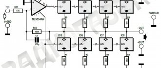
To improve the symmetry of the amplifier, the output stage is made of a complementary pair of transistors (Fig. 1):
Considering that the main parameters of the amplifier improve with increasing current transfer coefficient h21E. The output stage uses composite transistors KT827A (VT9) and KT825G (VT10), and the final stage of the linear amplifier (VT5) uses a composite transistor KT825G. To reduce nonlinear distortions of the “step” type, diodes VD5 and VD6 are included between the bases of transistors VT9, VT10. This ensures fairly reliable closing of the output stage transistors in the absence of a signal.
The input circuit has been slightly changed. The non-inverting input of op-amp DA1 was used as a signal input, which made it possible to increase the input resistance of the amplifier (it is determined by the resistance of resistor R1 and is equal to 100 kOhm). If high input resistance is not required, it is better to make the input circuit in accordance with the original. In this case, the input resistance will decrease to 22 kOhm, but the amplifier will become inverting and less prone to self-excitation when feedback occurs between its output and input (this connection will be negative). It should, however, be noted that even in the non-inverting version, the stability of the amplifier remains high.
To prevent clicks in the speakers caused by transient processes when turning on the power, as well as to protect the speakers from DC voltage when the amplifier or power supplies fail, a simple, well-proven device (VT6-VT8) is used, used in the industrial amplifier "Brig- 001". When this device is triggered, one of the lamps HL1, HL2 lights up, signaling the presence of a DC voltage of one polarity or another at the output of the amplifier. Replacing a lamp indicator with an LED one is described in the power supply diagram (see below). Otherwise, the circuit of the described amplifier does not differ from the circuit of the Kvod 405 amplifier.
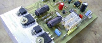
Unlike the original (Solntsevsky) version, each amplifier channel was assembled on a separate board (Fig. 2). Practice has shown that in this case it is easier to eliminate possible interference and interference from adjacent channels and the transformer.
Don't be intimidated by the size of the board. At the first inspection, a false impression of low installation density arises. Tests have shown that a number of elements get quite hot when the amplifier operates for a long time, and this configuration of the board promotes air circulation and cooling. In addition, it eliminates mutual interference between elements.
To connect to external circuits in the original version, MPH type connectors were used. If you want to struggle with soldering them (I didn’t have much fun soldering them), try it. I created the above drawing of the printed circuit board before meeting these connectors and, naturally, I was too lazy to redo it later. Yes, there is no point - you can solder wires into the same holes without any problems.
The circuit layout of the connector contacts is shown in the table:
| Address | PCB (connector) contacts |
| common wire | 1, 2, 7 |
| -27 V | 5, 6, 9, 20 |
| +27 V | 13, 14 |
| manifold VT10, manifold VT9 | 3, 4, 11, 12 |
| emitters VT9, VT10 | 18, 19 |
| VT10 base | 21 |
| VT9 | 22 |
| speaker | 15, 16 |
| faulty power supply indicator | 17 |
Amplifier Parts List
Chip:
- DA1 K574UD1A (I used it in a metal case)
Transistors:
- VT1, VT3, VT4 – KT3107B
- VT2 – KT3102B
- VT5 – KT825G
- VT6, VT8 – KT312V
- VT7 – KT608B
- VT9 – KT827A
- VT10 – KT825G
Resistors (I used resistors with a 5% tolerance):
- R1, R28 – 100 kOhm/0.25 W
- R2, R3, R24, R25, R26 – 10 kOhm/0.25 W
- R4 – 330 kOhm/0.25 W
- R5, R6 – 1 kOhm/0.25 W
- R7, R11, R13 – 3.3 kOhm/0.25 W
- R8 – 560 Ohm/0.25 W
- R9 – 22 kOhm/0.25 W
- R10 – 100 Ohm/0.25 W
- R12 – 180 Ohm/0.25 W
- R14 – 510 Ohm/0.25 W
- R15 – 270 Ohm/0.25 W
- R16 – 2.2 kOhm/0.25 W
- R17, R18, R19 – 1.5 kOhm/2 W
- R20 – 47 Ohm/0.5 W
- R21, R23 – 22 Ohm/0.25 W
- R22 – 10 Ohm/2 W
- R27 – 82 kOhm/0.25 W
- R29 – 6.8 kOhm/0.25 W
- R30 – 300 Ohm/0.25 W
- resistor for LED fault indicator 2.4 kOhm/0.5 W
Capacitors:
- S1 – KM 5B N90 0.15 µF
- C2, C7 – K53-18 100 µF/16 V (expensive tantalum capacitor. I installed a regular electrolyte without a noticeable loss of quality)
- C3, C4, C5, C6 – KM 5B N90 0.047 µF
- S8, S12 – K50-17B 330 pF
- S9 – K50-17B 100 pF
- S10 – tuning KT4-21B 4-22 pF
- S11 – K10-17B 91 pF
- S13, S16, S17 – K10-17B 0.1 µF
- S14, S15 – K50-29 220 µF/63 V with coaxial pinout
- S18 – K50-35 220 µF/10 V
- S19 – K50-35 68 uF/100 V
Diodes:
- VD3, VD4, VD5, VD6 – KD510A in glass
- VD7, VD8, VD9, VD10 – KD522B in glass
- two LEDs for the fault indicator: any at 10 mA.
Zener diodes:
- VD1, VD2 – KS515A in metal.
Relay:
- RES48A RS4.590.201.
I installed the transistors of the output stages (VT9, VT10) through dielectric spacers on radiators 150 mm long (sold in radio parts stores), 4 for each (1 radiator for 2 channels). VT5 transistors are installed without spacers on separate needle-shaped heat sinks mounted on the board.
An amplifier assembled from serviceable parts requires almost no adjustment. It is only necessary to select resistor R30 (for reliable operation of relay K1 a few seconds after turning on the power) and the total capacitance of capacitors C10, C11 (for minimum nonlinear distortion at a frequency of 20 kHz). The recommended method for selecting this capacitance in the original amplifier to minimize distortion of the output signal shape at frequencies of 50-100 kHz does not always give the desired result, so it is advisable to use it only in the absence of a nonlinear distortion meter.
Power supply
The schematic diagram of the power supply for the stereo version of the amplifier is shown in Fig. 3. It contains a T1 network transformer with four secondary windings and the same number of stabilized rectifiers. Two of them (G1 and G3) provide voltage of positive (relative to the common wire) polarity. The other two (G2 and G4) are negative. Each of the nodes G1 - G4, in turn, consists of a rectifier on diodes VD1 - VD4 (Fig. 3 shows a diagram of sources G1, G3), filter capacitors C1 - C4 and a voltage stabilizer on transistors VT1, VT2 and a zener diode V05. Stabilized voltage rectifiers of negative polarity (G2, G4) differ from those shown in Fig. 3 with the opposite polarity of the inclusion of diodes, zener diodes and electrolytic capacitors, as well as the transistors used (indicated in parentheses).
Voltage stabilizers are made according to a well-known circuit using transistors of different structures. Thanks to the inclusion of both transistors in a circuit with a common emitter, the parameters of such a device, despite its simplicity, are quite good. In addition, the stabilizers are resistant to overload and short circuits in the load. In the event of a short circuit, the zener diode VD5 is de-energized and transistors VT1, VT2 are closed. After the short circuit is eliminated, the device’s functionality is automatically restored. The stabilizers manufactured by the author were turned off at a load current of 7–8 A, which can be considered quite acceptable, since the current surge at the moment of breakdown of one of the transistors of the amplifier output stage exceeds this value.
As can be seen from the diagram, the regulating transistor VT2 is included in the “cold” (i.e., connected to the common wire of the amplifier) wire of the rectifier. This allows the control transistors of all four stabilizers to be installed on a common heat sink without any insulating spacers, and requires a separate transformer winding for each of the rectifiers.
The writing transformer is wound on a toroidal magnetic core OL100/50-50 with a cross-section of 12.5 cm2. Its winding 1 contains 880 turns of PEV-2 wire with a diameter of 0.86 mm, each of windings II-V contains 120 turns of PEV-2 wire with a diameter of 1.14 mm. To reduce external fields, and consequently, interference to circuits sensitive to such interference, the number of turns of the windings was chosen to be slightly larger than required by calculation. For the same purpose, an electrostatic screen (one layer of PEV-2 0.3 wire) is placed between the primary and secondary windings. The latter can also be wound with aluminum foil (for example, from high-capacity metal-paper capacitors), taking care, of course, to insulate its turns from each other and from the rest of the windings. A foil tape 10-20 mm wide, insulated on both sides with capacitor paper, is best suited.
If interference occurs from the transformer, you can shield it with sheet aluminum. I used a shield winding between the primary and secondary with a lead to ground.
If there is a transformer with only two suitable windings, the power supply circuit will have to be changed as follows: connect the terminals of 3 stabilizers to the common wire, use stabilized rectifiers G2, G4 (Fig. 2) as sources for positive polarity voltages (Fig. 2), and G1, G3 for negative ones. Naturally, in this case, VT2 transistors can be installed on a common heat sink only through insulating spacers.
Power Supply Parts List
Transistors:
- VT1 – KT3107V
- VT2 – KT826A
- VT1 * – KT3102B
- VT2 * – KT825G
Resistors (all with 5% tolerance):
- R1 – 3.6 kOhm/0.25 W
- R2 – 390 Ohm/2 W
- R3, R6 – 1.5 kOhm/0.5 W
- R4 – trimmer 330 Ohm (I selected the smallest one that was available)
- R5 – 470 Ohm/0.5 W
Capacitors:
- C1 – 4700 µF/63 V
- C2 – K53-18 22 µF/40 V (Expensive tantalum capacitor. I installed it, knowledgeable people say that it is useful for power supply. You can replace it with a cheap Chinese electrolyte at first).
Diodes:
- VD1, VD2, VD3, VD4 – KD213A
Zener diode:
- VD5 D818E in glass.
* – for boards with negative polarity.
Capacitor C1 is mounted on the board lying down (the height of the stabilizers is reduced significantly).
KD213A diodes (VD1 – VD4) are mounted without heat sinks. I installed the VT2 control transistors on the same radiator as the amplifier transistors (4 transistors each). In this case, it is desirable to connect the pins to the board with wires of a minimum length.
Coil design
The amplifier coils are wound in two layers on frames with a diameter of 10 and a length of 30 mm with PEV-2 1.0 wire and contain: L1 and L3 - 50 turns each (inductance 5-7 μH), L2 - 30 turns (3 μH). To reduce mutual coupling, coils L1 and L3 are installed perpendicular to one another and parallel to the board, and L2 is perpendicular to it. The winding length of coils L1 and L3 is 26 m, L2 – 18 mm. As the test showed, the coils can also be frameless. In this case, they are wound with the same wire under tension on a mandrel with a diameter of 9-10 mm. The rigidity of the coils removed from the mandrel is quite sufficient. If necessary, it can be increased by fastening the coils with a suitable glue or epoxy resin.
How to increase the nominal input voltage of the amplifier to 0.7 V? The easiest way to do this is to connect a resistor with a resistance of 200-390 kOhm in series with capacitor C1. The same goal can be achieved by reducing the cascade transmission coefficient at op-amp DA1. To do this, it is enough to increase the resistance of resistor R3 to 30-47 kOhm. When the op-amp self-excites, it is necessary to include a correction capacitor with a capacity of 5-30 pF between its pins 6 and 7.
Can the amplifier drive an 8 ohm load? Yes, it can, but its maximum output power in this case will be reduced to 35 W. The harmonic coefficient will decrease slightly.
Author of the amplifier: Solntsev Yu ., Moscow.
Editing the original article taking into account the modern elementary base: Green
[.pdf] version of the article.
High quality Class B amplifier
| Extended article by O. Reshetnikov edited by the journal Radio Yearbook - 1983. pp. 93-101 |
In recent years, a certain stereotype has developed in the circuit design of high-quality audio amplifiers.
Such an amplifier usually contains an input differential stage, a stage with a resistive load that amplifies the signal to the level required for normal operation of the output stage, a pre-terminal phase-inverted stage and a push-pull final stage with serial supply of transistors. To reduce distortion, the quiescent current of the final stage transistors is chosen to be quite large - often it is 250... 300 mA. At the same time, significant (up to tens of watts) power is dissipated on each of the transistors, which requires the use of effective heat sinks and the adoption of special measures to stabilize the thermal regime when the ambient temperature changes. Unfortunately, solving the last problem is often beyond the power of a radio amateur. The fact is that to ensure a constant quiescent current in the range of possible temperatures, the thermal resistance of the heat sink-medium must be quite definite. However, this is not so easy to achieve. The thermal resistance of a heat sink depends not only on its configuration, surface area and its processing, but also on the installation location in the amplifier case, and even (especially if the heat sink serves as the rear wall of the device, which often happens in practice) on the location of the amplifier in relation to other blocks of the sound-reproducing complex, to the walls of sectional furniture, the walls of the room, etc. It is not surprising that seemingly properly designed amateur LF amplifiers often cannot withstand long-term continuous operation, overheat and even fail.
Obviously, a radical means of increasing the thermal stability of the amplifier could be to transfer the final stage to mode B. However, this mode is characterized by large nonlinear distortions (such as a “step”), which, as was believed until recently, can only be eliminated by deep negative feedback (NFE), covering the entire amplifier. And this, generally speaking, is undesirable, since it entails the need to take special measures to combat the so-called dynamic intermodulation distortion that occurs in amplifiers with deep feedback.
But there are other ways to reduce the distortions inherent in mode B. We introduce one of them, which, by the way, is very promising, according to some experts, to the readers of the yearbook. We are talking about using so-called feedforward coupling (or forward coupling, as opposed to feedback, or backward coupling) to reduce distortion. Patented by Harold Black back in 1929 (by the way, he also owns a patent for negative feedback), this method of reducing distortion has not been used in sound reinforcement technology for decades, but recently it has increasingly attracted the attention of specialists as a very effective means of improving sound reproduction techniques. . Industrial amplifier models that use direct coupling have appeared on the world market. One of them is a powerful audio amplifier “ Kvod 405”
", created by English. With a relatively simple circuit design, the developers managed to increase the harmonic distortion at mid frequencies to 0.005%.
Functional diagram of the amplifier “ Kvod 405”
» is shown in Fig. 1. Here A1 is an idealized amplifier that provides signal amplification to the level required for normal operation of the output stage, Vl and V2 are a complementary pair of transistors of the output stage operating in mode B, elements Rl, C1, R2 and L1 are the shoulders of a variable bridge calculated in a certain way current, RC and RH - respectively, the resistance of the signal source and the amplifier load. The principle of reducing distortion in such an amplifier becomes clear from the analysis of the dependence connecting the load voltage uH with the signal voltage uC and the base current ib of the output stage transistors. This dependence can be represented in the form uH = AuC + Bib, where A and B are some coefficients, the numerical values of which are determined by the parameters of the elements included in the device. Obviously, the main source of distortion can only be the base current ib, so you can get rid of them by selecting the parameters of the elements so that the coefficient B becomes equal to zero. By expressing coefficient B through the parameters of the bridge elements, it is easy to show that the condition of absence (compensation) of distortion coincides with the condition of bridge balance, i.e. L1/C1=R1/R2 In other words, by balancing the bridge at any frequency, you can guarantee that over the entire operating frequency range, the distortion introduced by the amplifier will be minimal.
What is the mechanism for compensating for distortion in this case? Simplified, it can be represented as follows. As is known from the theory of electrical circuits, a balanced AC bridge has the property that an alternating voltage applied to one of its diagonals cannot cause a potential difference to appear in the other diagonal. A similar picture is observed here: the distortion voltage that occurs in the output stage on transistors V1, V2 is applied to the BD diagonal, so it cannot appear in the other diagonal - AC. If, in addition to this, we assume that amplifier A1 has an infinitely large gain, then we can assume that point A is actually connected to the common wire (i.e., to the lower - according to the diagram - load terminal RH) and, therefore, there will be no distortion and under load. Thanks to resistor R2, nonlinear products in the spectrum of output current i1 are compensated by “pumping” the correcting current i2 directly from the output of linear amplifier A1 to the load, and higher harmonics are most effectively compensated, which is due in this case to the choice of resistor resistance from the condition of equality of currents i1 and i2 at high frequencies.
The complete circuit diagram of the amplifier, made on a domestic element base by Muscovite O. Reshetnikov, is shown in Fig. 2. The technical characteristics of the amplifier obtained by him are as follows:
| Nominal range of reproduced frequencies, Hz, with frequency response unevenness ±1 dB | 20…20 000 |
| Output power in the nominal frequency range, W, into a load of 8 Ohms with a harmonic coefficient of no more than 0.02% | 30 |
| The same with a 4 ohm load | 40 |
| Sensitivity, V | 0,2 |
| Input impedance, kOhm | 20 |
| Relative noise level, dB | -75 |
Along with low nonlinear distortions, the amplifier is distinguished by a very low level of dynamic intermodulation distortion, achieved by using frequency response correction. In addition, as already mentioned, the distortion compensation method itself, used in the amplifier, provides the most effective suppression of precisely higher harmonics, which are usually classified as dynamic distortions.
The linear part of the amplification path (amplifier A1 in Fig. 1) is made of operational amplifier (OP) A1 and transistors V3 - V6, V9, the final stage operating in mode B is made of transistors V12 and V15, V16. Transistors V7 and V13 are used in the device for protecting the final stage from overcurrent and short circuit in the load. The amplifier is powered by a simple bipolar rectifier using diodes V17-V20 with a capacitive filter made of large capacitors.
The gain of the cascade on op-amp A1 is determined by the parameters of the elements of the surrounding circuit OOS C1R2R5C3 and in the nominal frequency range is approximately 15. The use of an op-amp and deep OOS for direct current from the output of the amplifier to its inverting input made it possible to minimize the direct voltage at amplifier output. The first stage is powered by stabilized voltages taken from the zener diodes V1 and V2.
The second stage of the amplifier is assembled on transistor V4 with a current source on transistor V3, the use of which made it possible to obtain the maximum possible voltage gain in this case. The following double emitter follower on transistors V5, V6 serves to match with the last stage of the linear amplifier, made on transistor V9. From the output of this stage, the amplified signal goes to the final stage (V12, V15, VI6), and from it to the load.
The bridge elements in this amplifier are resistors R15, R29, capacitor C6 and coil L1. By selecting capacitor C6, the bridge is balanced at high frequencies, so high-frequency distortion products are compensated by the correcting current flowing into the load through resistor R29. In the region of lower frequencies, due to the finite resistance of the coil wire L1 (it cannot be reduced to zero), the balance of the bridge is disrupted. To reduce distortion at these frequencies, a deep (50...70 dB) OOS has been introduced, the voltage of which is removed from the output of the amplifier and fed through the divider R12R15 into the emitter circuit of transistor V4.
Elements R30, L2, R31, SP-C13 prevent self-excitation of the amplifier, capacitors C6-C8 provide correction of its frequency response in order to minimize dynamic distortion.
The protection devices for both arms of the amplifier are made identically. Each of them consists of a controlled resistor (transistors V7, V13) and a voltage divider (R21R18R20R26 and R23R19R22R27). The current limitation through transistor V12 of the upper arm of the final stage according to the diagram occurs as follows. In the absence of a signal, a current flows through the divider R21R18R20R26, determined by the voltage applied to it (24 V). This current (approximately 6 mA) creates a voltage drop of about 0.45 V across resistors R20 and R26, so transistor V7 is turned off. With the advent of the amplified signal, this voltage drop begins to change: during time intervals when the signal voltage changes in a positive direction, the voltage drop across resistor R20 decreases (due to a decrease in the voltage applied to resistors R21, R18, R20), and across resistor R26 ( it is mainly due to the collector current of transistor V12) - increases. At the moment when the total voltage drop across resistors R20 and R26 reaches a value of approximately 0.65 V, the protection transistor V7 begins to open and the resistance of its emitter-collector section shunts the input of the amplifier stage on transistor V9, thereby limiting the increase in current through transistor V12. Similar processes occur in the lower arm of the amplifier in the circuit when the signal voltage changes in the negative direction, but in this case, the emitter-collector section of transistor V13 bypasses the input of the stage on transistor V15. Diodes V8, V14 prevent the protection from reacting to an increase in the voltage drop across resistors R20 and R22 at moments when the signal voltage changes in the opposite direction (negative for the upper and positive for the lower arm) side.
With the values of resistors R18 - R23, R26, R27 indicated on the circuit diagram, the current limitation of the transistors of the final stage occurs at a value of about 3.5 A. The protection responds to a short circuit in the load by limiting the current at 1.5 A.
The amplifier can use operational amplifiers K140UD7, 153UD6 (most desirable, since the latter has a reduced noise level), transistors KT342G, KT315G, KT315D, KT315E (V4), KT361V, KT361D (V3, V5-V7, V13); diodes KD10ZA and KD504A can be replaced with any silicon diodes, respectively designed for forward currents of 10 and 50 mA. In the absence of KS515A zener diodes, it is possible to use D814A zener diodes connected in series and selected so that the total (on each pair) stabilization voltage is 15 V.
A possible version of the amplifier printed circuit board is shown in Fig. 3. It is designed for the installation of MLT resistors, KM capacitors (C1, SZ, C5, C10-C13), KSO-1 (C6-C8), K53-1 (C9) and K50-6 (C2, C4). Resistors R26, R27 are pieces of constantan wire with a diameter of 0.3 mm. Coils L1 (30 turns) and L2 (46 turns) are wound turn to turn in two layers on organic glass frames with a diameter of 7 and a length of 35 mm; the first with a bundle of 20 PEV-2 0.23 wires, the second with a PEV-2 1.0 wire (its inductance can be in the range of 4.9...8.8 μH).
Transistors V9, V12, V15 and V16 are installed on a common heat sink with a cooling surface of 800...900 cm2 and isolated from it with mica gaskets 0.1 mm thick. You should not install transistors on separate heat sinks isolated from each other and from the amplifier body, as is recommended to improve the thermal conditions of the transistors (in this case they are mounted without insulating gaskets). On the one hand, this is not particularly necessary, since of all the transistors only transistor V9 heats up significantly (the power dissipated on it is about 1.2 W), on the other hand, such an installation of the output stage can lead to self-excitation of the amplifier at high levels that is difficult to eliminate ( on the order of several megahertz) frequencies. To avoid self-excitation, the transistors on the heat sink and the board in relation to it must be positioned so that the connecting wires are as short as possible. To facilitate the thermal regime of transistor V4 (the power dissipated on it is approximately 100 mW), it is advisable to tightly place an aluminum or copper heat sink on its body in the form of a small (approximately 20×20 mm) plate with a thickness of 4...5 mm.
The amplifier power transformer, manufactured by O. Reshetnikov, is wound on a toroidal magnetic core with an outer diameter of 100, an inner diameter of 64 and a height of 32 mm. The primary winding (1130 turns) is wound with PEV-2 0.5 wire, the secondary winding (2×10⁴ turns) is wound with PEV-2 1.3 wire, the electrostatic screen between them is with PEV-2 0.21 wire (one layer). Filter capacitors C14, C15—K50-18. In the absence of a toroidal magnetic core, you can use a W-shaped magnetic core with a cross section of 8...10 cm2, the window of which will allow you to place windings from the specified wire. The capacitance of the anti-aliasing filter capacitors can be reduced to 4000 µF.
approx. here a table of currents and voltages on transistors will be added
An amplifier assembled from serviceable parts is not difficult to set up. It is only necessary, when working on an equivalent load, to check the transistor modes for compliance with those given in the table (voltage deviations within ±20% are permissible) and balance the R15C6R29L1 bridge to minimize output signal distortion. The last operation is best performed by viewing on the oscilloscope screen the output signal remaining after suppression of the first harmonic, or the difference signal obtained by compensating the output signal with the input signal. In the latter case, it is very convenient to use the device described by I. Akulinichev in the article “Attachment to an oscilloscope for assessing the quality of amplifiers” (“Radio”, 1980, No. 4, p. 40). Balance the bridge at a frequency of 10...12 kHz by selecting capacitor C6 until minimal bursts are obtained in the signal oscillogram. Balancing can also be done using the oscillogram of the unsuppressed output signal. In this case, its frequency is increased to 50... 100 kHz and minimal signal distortion is achieved by selecting the same capacitor. Improved balancing at low frequencies can be achieved by shunting capacitor C6 with a resistor with a resistance of several hundred kilo-ohms.
If desired, the output power of the amplifier can be increased to 60...80 W. To do this, it is necessary to increase the supply voltage to 35...40 V and replace the transistors of the final stage with KT803A. To maintain current modes (transistors V4 and V9), the resistance of resistor R9 must be reduced to 620..750 Ohms, and resistors R24, R25 must be increased to 430...510 Ohms. In addition, it is necessary to raise the response threshold of overcurrent protection devices, for which reduce the resistance of resistors R26, R27 to 0.1 ... 0.11 Ohms and increase the resistance of resistors R21, R23 to 8.2 ... 10 kOhm. By the way, the selection of resistors for protection devices is necessary in any case if the supply voltage differs from that indicated in the diagram.
The dynamic range of an amplifier can be expanded by reducing its sensitivity, which in many cases turns out to be excessive. This is not difficult to do - it is enough to select elements C1, R2, R5, SZ to increase the depth of the OOS covering op-amp A1. For example, to reduce the sensitivity of the amplifier to 0.7 V, it is necessary to reduce the resistance of resistors R5 to 100 kOhm, and increase the capacitance of capacitor SZ to 0.15 μF.
Source:
High quality Class B amplifier. Radio Yearbook 1983. pp. 93-101