Op Amps Review
Posted on 28th Jan 2022 in Professional Audio
For a simple and convenient selection of operational amplifiers, I have compiled a table
Before describing the sound and my impressions, I will write a list of operational amplifiers that I installed in my studio card, mixing console and listened to from 2022 to 2022:
- opa2134
- opa134
- opa1611
- opa2211
- opa211
- opa2604
- opa2227
- lme49720
- lm6172
- lm6171
- opa827
- ada4627
- ad8512
- ad797
- ad8676
- op27
- lm837
- tl072
- tl052
- tl032
- mc33078
- ne5532
- ne5534
- k544ud1a
- lf353
- ths3111
- njm2068
- njm4560
- njm4558
I’ll immediately answer the main question that arises in your mind: there is no best opamp; there are combinations in which each of them has a better role. Now a little more detail.
The first thing that fundamentally affects the sound of an operational amplifier is the quality of the power supply; with a switching power supply, you can expect good sound only from slow operational amplifiers with a slew rate of less than 9V/μs , such as ne5532 , njm2068 , njm4558 , njm4560 , op27 , others more fast op-amps will sound too dull and pale. Plus, at a minimum, such a power supply requires high-quality Nichicon PW (not only me, but also the engineers of the Black Lion ).
The slew rate of the signal is a parameter of the operational amplifier equal to the color of the sound in relation to its detail, in other words, the lower the speed, the greater the pleasant transistor color and the less detail, and vice versa, the higher the speed of the op-amp, the greater the detail and 3D effect, but at the same time the sound becomes dry and sterile. Therefore, studio equipment manufacturers such as SSL , Black Lion , Digidesign , AVID use combinations of fast and slow operational amplifiers in their devices; in such combinations, the sound appears quite detailed and, at the same time, bright and lively.
Op-amps based on bipolar transistors sound as detailed as possible, but at the same time rather dry. Op amps with FET sound less detailed but produce a wetter, warmer sound. This gives the following principle for using op-amps: you cannot use only op-amps based on bipolar transistors or only op-amps with field-effect transistors at the input. Combinations are a must if you're looking for the coolest sound possible.
Conclusion - all hi-end and studio devices of high class and sound quality using op-amps are built on a combination of fast operational amplifiers on bipolar transistors (with a speed of more than 9) with slow field-effect amplifiers (with a speed of less than 9) or vice versa on a combination of fast operational amplifiers on field-effect transistors (more than 20) with slow ones on bipolar ones (less than 9).
Plus, among equals, a device with a better power supply with a good transformer and high-quality capacitors
ne5532 is rightfully the king among operational amplifiers based on bipolar transistors, due to its low speed of 9V/µs it does not have the highest detail, and due to it it also has a very pleasant transistor sound, gives good amplification and a sound picture right in front of your face, every element of the music is larger and closer to the listener. All this is only subject to the correct power supply circuit - two electrolytes of at least 100 μF from the plus and minus of the power supply to ground and three 0.1 μF ceramic capacitors from plus to minus to ground and between the plus and minus of the power supply. In combination with the tl072 as an integrator (dc servo), it gives the legendary sound of classic English studio consoles (mixing consoles).
opa2134 (opa134) is a beloved operational amplifier with a speed of 20V/µs - its secret is distortion in the form of a bunch of harmonics at mid and high frequencies, that the sound has a very warm tube mid and top, it is thanks to such features that it gives what is more no other operational amplifier with similar characteristics can provide, and that is why such manufacturers as Digidesign , AVID , Dangerous , Black lion . Pro tools HD interfaces with integrators (dc servo) on slow opa2227 .
ada4627 - clear as a baby's tear in sound, a fast 82V/µs operational amplifier with field-effect transistors at the input, there is a slight feeling of sterility of the sound due to the very high speed, therefore it necessarily requires a slow integrator (dc servo) on bipolar transistors with a speed below 9V/µs , for example, such as opa2227 .
opa827 - similar to the ada4627 op amp, both in sound and characteristics, lagging behind in clarity and volume, due to the low 28V/μs speed relative to the ada4627 . The advantages include working with power supply up to +-18V , while ada4627 only works with supply voltage up to +-15V . To most people who test and use opa827, it seems more boring in sound than opa627 (55V/µs) and perhaps this is also due to the difference in speeds. To my ears, it also did not stand out in terms of sound color, it gave a small (not particularly amplified) moistened but uncolored sound - in short, it reminded me of a slightly muddy version of ada4627 .
ad8512 is a fairly fast op-amp based on field-effect transistors with a speed of 20V/µs , which has a sound similar to opa827 , perhaps the sound feels larger in size than that of opa827 due to a different construction circuit, and I can say that it quite pleasantly moisturizes the sound due to its construction on field-effect transistors . Jim Williams , the guru of American sound studio and hi-end instrumentation, recommended using it as an integrator (dc servo) when upgrading the tl072 in studio equipment, and I followed this recommendation - the sound became quite clearer and wetter compared to the tl072 , but the color clearly decreased and I have to think how to add color and what else can be changed in the scheme. Well, so that you finally understand the full power of this op-amp, I will add that it is used in the best studio reverb of our time, Bricasti M7 .
lm6172 (lm6171) 3000V/μs operational amplifier that is a reference in terms of detail and clarity of sound creates a maximum 3D effect , requires high-quality power supply with tantalum capacitors from plus and minus to ground and not only (see datasheet), the best option for output op-amps ( output buffer) for all audio devices, of course, has the disadvantage of seriously drying out the sound and, as I already wrote, requires combination with slow op-amps (integrators (dc servo) or other combinations), preferably with a field-effect transistor input, such as tl072 or tl032 .
ths3111 - similar to lm6171 high-speed op-amp 1300V/µs , inferior to it in speed, and for the same reason inferior in detail and volume of sound. It is this operational amplifier that is used as a preamplifier signal directly from the output of the DAC in the Digidesign 192io (yes, I have the circuit and the interface itself) of the Pro-tools HD .
opa2227 is the antipode of lm6172, the slowest 2V/µs and therefore the most colorful and brightly colored op-amp with great sound and therefore is rightfully considered one of the best op-amps for use as an integrator (dc servo) with many fast op-amps with field-effect transistor inputs, such as ada4627 , opa2134 , opa134 , opa827 , opa627 .
opa1611 is a fairly recent op-amp, actively tested by everyone who is not afraid of SOIC soldering, in comparison with the ne5532 it is more detailed, with less gain and without the approximation effect like the 5532 , but it immediately allows you to see all the reflections of the reverbs, all the little details of the effects and even distortions and jambs of the recording, not as sharp as with lm6172 but much clearer, naturally the speed of 27V/μs also gives an obvious drawback - the sound is pale, sterile, without color, therefore without an integrator (dc servo) like tl032 this op-amp will not be pleasant to you, it will be detailed and analytical, but boring, and only a slow op-amp with a field input can breathe life into it. In my console, the good old tl072 with 13V/µs also performed the role of an integrator well, but still a slower op-amp would be preferable. Plus I forgot to add that opa1611 significantly adds bass in comparison with ne5532 and removes vocals.
The tl072 is truly a multi-platinum op amp in the dc servo role, used even in all other possible roles in Soundcraft , Allen & Heath and the great SSL . Why don't other roles suit him well? Well, nowadays it sounds, frankly speaking, as pleasant as it is huge and just as muddy. This is a really big wet warm but muddy sound (since the op-amp is not the fastest 13V/µs and also with field-effect transistors), so it ideally complements the more or less detailed, slightly fast op-amps on bipolar transistors, and the ideal pair for it would be the ne5532 , not bad as I said it works with my opa1611 and opa211 adding colors and dimensions to their detail. Almost an analogue of tl072 is lf353 both in characteristics and in sound, but lf353 is designed for stable operation at +-18 volts , and tl072 at +-15 volts .
tl032 - maximum color bright slow 3-5V/µs op amp used as an integrator (dc servo) in most modern SSL . For me this is the most understandable description.
opa2604 is an operational amplifier with field-effect transistors at the input, underestimated by many, and at the same time giving a moistened, fairly clear sound, when supplied with capacitors similar to those in the ne5532 , among Western pros it is considered one of the best for use in the I/U role. SSL consoles in this very role of a current/voltage converter, starting with the SSL9000 .
lme49710 (lme49720) is a fast precision op-amp (20V/µs), widely used to upgrade the ne5532 or in combination with it. In combination with ne5532 it is used in many modern audio cards such as ASUS Essence STX II , where the slow ne5532 is used to set the color and bring closer (increase) the sound and lme49720 to speed up the sound and good sound of highs and more liveliness, naturally, since both of these op-amps on bipolar transistors the sound is a bit dry and most of those who start upgrading these cards change lme49720 to opa2132 or opa2134 . In studio technology, the lme49720 is successfully used in new models of audient , and so that the sound does not seem a bit dry due to their speed (and the bipolar transistors on which the lme49720 ), in these consoles it is used in conjunction with input audio transformers that provide a good share of saturation and harmonics. It is very important to know that you definitely won’t like the sound of this op-amp, like many other high-speed ones, if you forget to put electrolytes from 10 microfarads or more into the power supply from plus and minus to ground, or if they are not provided in advance in the device where you are planning upgrade - this is stated in the datasheet (passport) of the OU.
The article is being updated...
Also read
Aronov op amp selection table
The table shows the main characteristics of operational amplifiers that affect...
Facebook Twitter Vkontakte
Maxim Aronov
Sound Specialist and itBlog Comments powered by Disqus.
WHAT IS AN OPERATIONAL AMPLIFIERAPPLICATION OF OPERATIONAL AMPLIFIER IN AUDIO ENGINEERING
BEGINNING OF ARTICLE
However, op-amps are good not only in buffer amplifiers - using sets of resistors and capacitors, you can build tone controls, multi-band equalizers, and filters only for a certain frequency range. For example, consider the diagram in Figure 29:
Figure 29. High-pass filter.
R1 and C2 form a first-order filter, the principle of which is better explained in terms of reactance - when a certain frequency is reached, the reactance will begin to decrease and as soon as it becomes significantly less than R1, the amplitude of the input signal will also begin to decrease. To check, let’s take the frequency response of this circuit, drawn by the simulator:
Figure 30.
Now let's recalculate the reactance C1 for the frequencies shown in the graph above. The bending of the frequency response line begins at approximately 2 kHz, for this frequency the reactance of C2 will be 169 kOhm, in relation to 22 kOhm of R1 this begins to be felt. At a frequency of 24.1 kHz, resistance C2 will be 14 kOhm and this is already 1.6 times less than resistance R1, therefore the voltage should also decrease by 1.6 times, which actually happens at a voltage of 1.22 V at a low frequency of 500 Hz at a frequency of 24 kHz the amplitude decreased to 0.75 V, i.e. the same 1.6 times. Now let’s add one more link, exactly the same as R1-C2, and get a second-order filter:
Figure 31. Second-order filter Figure 32. Frequency response of a second-order filter.
As can be seen from the figure, the output voltage at low frequencies has decreased, literally by 0.2 V, but at high frequencies the rollover occurs much more intensely - now at a frequency of 24 kHz the output voltage is 0.3 V, which is more than 2 times less than in the previous filter. For greater clarity, convert these values into dB, since the human ear perceives the volume level according to the logarithmic law, and the frequency response of a third-order filter takes the following form:
Figure33. Frequency response of the second order filter in dB.
From the graph it is now clear that at a frequency of 24 kHz the frequency response rolloff is 10 dB, i.e. 3 times lower than the low frequency. The quality factor of this filter, i.e. the dependence on how much the gain will decrease depending on the change in frequency is 5 dB per octave. Octave is a musical concept that means that the frequency has changed exactly 2 times. In this case, frequencies of 10 kHz and 20 kHz were taken as the segment for calculations; in this section, the amplitude decreased by 5.2 dB. Let's consider another example - a third-order filter, i.e. containing 3 identical nodes:
Figure 34. Third order filter. Figure 35. Frequency response of a third-order filter.
In this filter, the frequency response rolloff is 7.5 dB per octave, i.e. The decrease in amplitude occurs much more intensely. Using the same principle, you can organize low-pass filters:
Figure 36. Low-pass filter Figure 37. Frequency response of the low-pass filter
These filters are commonly used in complete power amplifiers to limit the edges of the audio range where unpleasant interference tends to reside. However, using the circuitry of a high-pass filter, you can organize a low-pass filter for a subwoofer:
Figure 38. Filter for a subwoofer Figure 39. Frequency response of a filter for a subwoofer
Despite the full functionality of this filter, it would not be entirely correct to recommend its use - it has no limitation in the infra-low frequencies, and this increases the chance of overheating of the dynamic head coil or its mechanical damage from impacts on the magnetic system. Now consider the following scheme as a filter:
Figure 40.
Here the op-amp is connected through an inverting input, and the op-amp OOS contains RC circuits that will definitely affect the frequency response of this circuit. The circuit also contains a variable resistor X1, with the engine in the middle position, the components of the OOS and input circuit are made completely symmetrical, which gives the right to assume that the OOS compensates for changes in the frequency response that the input elements will make. On the diagram to the left of the engine is written the resistor value, in this case it is 100 kOhm, and to the right is the position of the engine as a percentage relative to its full stroke, i.e. 50 means the engine is in the middle. To check the judgments about the frequency response, let's look at the frequency response of this circuit generated by the simulator:
Figure 41.
Indeed, the red line displaying the shape of the frequency response practically follows the zero mark. Now let’s move the variable resistor slider towards R2:
Figure 42.
As can be seen from the figure, the amplifier began to amplify a certain section of the frequency response, located in the region of 40 Hz, and this indicates that the reactance of capacitors C2 and C3 changes so much that it begins to affect the environmental feedback, and the shape of the resulting frequency response strongly resembles the shape of the frequency response of an LC resonant circuit , however, there are no inductances here, therefore resonance as such is not possible. To determine the burst frequency, an additional concept is introduced - QUASIRESONANCE. Quasi-resonance can cause either a surge in the frequency response up or a drop down - just move the variable resistor slider towards R4:
Figure 43
Using this filter, you can already create a full-fledged filter for a subwoofer, since it has good limitations in the infra-low frequencies. The only thing that may be required is to change the value of the frequency-setting capacitors, since the quality factor of the filter is quite high. The result is the following circuit and its frequency response:
Figure 44
Using several filters connected in parallel, but having different frequency-setting capacitors, you can build an equalizer - a tone control that makes adjustments in four or more frequency response sections (bands). Figure 45 shows a diagram of such an 8-band equalizer:
Figure 45. Schematic diagram of an 8-band equalizer.
However, this is far from the only way to build equalizers using op-amps. Figure 47 shows a diagram of a completely passive equalizer, in which op-amps act as a buffer amplifier (X1) and a loss compensator (X2).
Figure 46. Schematic diagram of a passive equalizer published in RADIO magazine in the eighties.
Sometimes, to build equalizers based on an op-amp, separate bandpass filters are used, included in the OOS of another op-amp. This makes it possible to reduce the influence of the bands on each other, as well as to change over a wide range the values of the rise and fall of the frequency response section of the selected band:
Figure 47.
However, when building a stereo equalizer, it is desirable that both channels are identical to each other, and this requires the use of both resistors and capacitors without variation in parameters. It is very difficult to find such ones, so you have to select both resistors and capacitors. A change in the circuit design of bandpass filters, namely the use of adjustable filters, will allow you to get rid of this trouble. In the eighties, RADIO published a diagram of a similar equalizer based on the K157UD2. The use of these particular op-amps was justified by the fact that they are dual. However, today there is no shortage of microcircuits containing 4 op-amps in their package, therefore, an increase in the number of op-amps for adjustable filters will have virtually no effect on the increase in the number of microcircuits. A diagram of a five-band equalizer based on adjustable filters is shown in Figure 48, and this equalizer can easily be expanded to 15 bands:
Figure 48.
By the way, all the equalizers proposed above were of the graphic variety, i.e. When using slider variable resistors, apply a calibration near each slider, then by the position of the resistor slider you can judge the shape of the frequency response:
Figure 49. Front panel of the graphic equalizer PRIBOI E024S
However, there is another type of equalizer - parametric. These equalizers allow you to influence not only the rise and fall of the frequency response in a certain area, but also move this area and, in addition, adjust the quality factor.
Figure 50. Front panel of the Klark Teknik DN410 parametric equalizer
In everyday life, such equalizers are used extremely rarely, however, they allow you to more accurately adjust the frequency response depending on the need. We are actually talking about parametric equalizers because the circuit in Figure 48 allows you to transform this equalizer into a parametric one, for which it is necessary to replace the trimming resistors of the bandpass filters with a series-connected trimming resistor of a lower value and a variable resistor located on the front panel. On the other hand, no one forbids using one band of this equalizer to isolate and enhance a narrow section of the frequency response, which is precisely what is necessary to create a multifunctional filter for a subwoofer, to which all that remains is to add a phase shifter to eliminate the phase change occurring in the filter itself. The result is the following filter circuit for the subwoofer:
Figure 51. Schematic diagram of a subwoofer filter.
Figures 52 and 53 show changes in the shape of the frequency response depending on the adjustment of frequency and quality factor:
Figure 52. Changing the filter frequency for the subwoofer Figure 53. Changing the quality factor of the subwoofer filter.
All previously considered options for using op amps were based on the use of negative feedback feedback. However, the op-amp can also be covered by positive feedback - POS, i.e. feedback is sent to the NON-INVERTING INPUT. This inclusion allows you to “digitize” some analog events, for example, when a certain temperature is reached, some event should occur, for example, a forced cooling fan should turn on, and as soon as the temperature drops below a certain temperature, it should turn off. Similar actions can be carried out by the fan control circuit shown in Figure 54.
Figure 54. Schematic diagram of fan control.
In the diagram, R7 acts as a computer fan, the size and performance of which depend on the design of the amplifier. The tuning resistor X1 adjusts the response threshold of the thermostat. Resistor R8 is used to turn on the fan at minimum speed and must have a power of at least 1 W, and the resistance is selected depending on the performance. For greater clarity, let’s connect a low-frequency generator with a small amplitude to the circuit, simulating a change in R2 depending on temperature, and compare the input and output voltages of the op-amp:
Figure 55. Op-amp input and output voltages.
Here the blue line indicates the input voltage at the inverting input, the red line at the non-inverting input, and the green line at the output of the op-amp. Since the output voltage changes, through resistor R4 it also affects the voltage value at the non-inverting input, however, in this figure the dependence of the changes is not very clearly visible, so let’s turn off the voltage at the output of the op-amp and take a closer look at the voltages at the inputs:
Figure 56. Op-amp input voltage.
While the thermistor R2 is cold, its resistance is high and the voltage at the inverting input will be positive, therefore the voltage at the output of the op-amp will be as close as possible to the negative supply voltage (blue line in Figure 56), and this in turn will lead to the appearance of a small negative voltage at the non-inverting input, approximately -0.3 V (red line in Figure 56). As R2 heats up, its resistance will begin to decrease, which will result in a decrease in the voltage at the inverting input of the op-amp, and then a transition to a negative value. As soon as the voltage at the inverting input becomes less than at the non-inverting input, the voltage value at the output of the op-amp will begin to increase, which will entail an increase in the voltage at the non-inverting input and the voltage difference at the inputs of the op-amp will increase even more. Since the op-amp amplifies only the voltage difference at the inverting and non-inverting inputs, an increase in the voltage difference will entail an even greater increase in the output voltage at the output of the op-amp and the difference in input voltages will become even greater. In this way, an avalanche process is formed, which contributes to an almost instantaneous change in the output voltage at the output of the op-amp, which actually happens in Figure 56, at point 1 of the time scale. At the end of this process, a voltage is formed at the output of the op-amp, close in value to the positive power source, and a positive voltage of 0.3 V appears at the non-inverting input. The appearance of a positive voltage at the output of the op-amp opens transistor Q1 (2N5551), which in turn opens Q2 (BD139) and the fan increases speed to maximum. By the way, a voltage of almost 15 V cannot be supplied to all computer fans, since not all fans have a motor winding control device that allows them to operate at higher speeds. When the maximum speed is reached and the supply voltage is further increased, the magnetic field of the glued magnets of the engine already has time to “overshoot” the desired Hall sensor and as a result, engine vibration increases, the speed drops and the heating of the engine power switches sharply increases. Therefore, when powering the circuit from a voltage of ±15 V, a 0.5 W resistor should be provided in series with the fan. The resistance of this resistor is selected in such a way that there is 12-13 V on the fan, usually 5...10 Ohms is enough. As soon as cooling has begun, logically, the resistance of the thermistor should increase, but let's assume that the thermal resistance of the radiator is not very good and the thermistor continues to heat up, and the voltage at the inverting input continues to decrease. But after some time, the thermistor will begin to cool and its resistance will begin to increase, and the voltage at the inverting input will begin to increase, reach zero and become a positive value. As soon as the voltage reaches a value equal to the voltage at the non-inverting input and an avalanche process will immediately begin, but in the negative direction - the output will begin to decrease, causing a decrease in the voltage at the non-inverting input, increasing the voltage difference at the input of the op-amp and eventually approaching the voltage as much as possible negative supply voltage. This is what actually happens at time point 2, at which the fan turns off. As can be seen from the graph, the switching of the op-amp does not occur at the same temperature - first there should be a slight overheating (the voltage on the thermistor should become less than -0.3 V), relative to the set value, and then slight overcooling (the voltage on the thermistor should exceed +0.3 V). Based on this, you can build the graph shown in Figure 57:
Figure 57.
The resulting circuit represents one of the possible implementations of a Schmitt trigger or comparator, and the graph presented in Figure 57 is a description of the Hysteresis loop, i.e. This circuit can be considered as the simplest analog-to-digital converter - ADC. In addition to temperature control, similar comparator circuits can be used to control the second power level in powerful class H audio amplifiers. The operating principle of these amplifiers is based on dividing the supply voltage into two, usually equal parts, and as long as the output signal level is less than the lower power supply, the final stage uses namely a low voltage source. As soon as the amplitude of the output signal begins to approach the value of the supply voltage, the “second part” of the supply is supplied to the final stage. For a more detailed look, we use the Holton amplifier:
Figure 58. Holton circuit diagram for Class H.
In this circuit, a specialized op-amp LM311 is used as a comparator, which has a transistor at the output and an output emitter and collector, which significantly expands the capabilities of this microcircuit - it is possible to turn on both a repeater and an open-collector output. As soon as the voltage at the output of the amplifier reaches +40 V, comparator X3 will change the voltage at its output and transistors X9 and X10 will open and a voltage of +100 V will be applied to the drains of the transistors of the final stage. As soon as the output voltage drops below 22 V, the comparator will change its state again and the “second floor” of the power supply will be turned off. The voltage at which the “second floor” of power is connected and turned off is determined by the position of the trimmer resistor R30, and the Hysteresis loop is formed by resistor R37 and in this circuit the value of this resistor is slightly underestimated for greater clarity. When repeating the circuit, it is recommended to use a 2.2 MΩ rating. If you are confident that you have the CORRECT layout of the printed circuit board and the likelihood of impulse interference is reduced to a minimum, then you can completely abandon this resistor - the internal structure of the microcircuit allows it. For the negative arm, the same process occurs, only it is monitored by a comparator on X4, and the second power level is connected to transistors M7 and M8.
Figure 59. Control of the second power level of a Class H amplifier.
IRF640 and IRF9640, as the most common ones, are used as transistors for connecting the second power level in the circuit. Resistors R63, R64, R69, R71 are used to reduce the shock process that occurs when the second-level transistors open and which inevitably appears on the output signal. To reduce this same process, capacitors C13 and C14 are also used. If there are no problems with the configuration, then instead of pairs of power transistors, you can use higher current transistors IRF5210 for the positive arm and IRF3710 for the negative one, one at a time. Resistors in the sources must be reduced to 0.1 Ohm. The control systems are powered by parametric stabilizers R53-D8-D9, for the positive power supply arm, and R56-D10-D11, for the negative arm. Two identical zener diodes provide a virtual midpoint for each op-amp, and this point is the reference point for the operation of the comparator. Well, what exactly does such inclusion of the final stage give? First of all, reducing the heat dissipated by the final cascade, since changing the supply voltage of the final cascade significantly reduces the body dissipated by this cascade. And since the heat generated has become significantly less, it is already possible to use fewer pairs of transistors for this very final stage, and this already saves money. In addition, IRFP240-IRFP9240 are used as final stage transistors, the maximum DRAIN-SOURCE voltage is 200 V, therefore the amplifier supply voltage according to the traditional circuit should not exceed ±90 V (ten volts for the technological margin, although this is not enough). Using a two-level power supply, the voltage can be increased, since at any time no more than 3/4 of the total supply voltage will be applied to the transistors. In other words, even when powered by a two-level supply of ±50 V and ±100 V, a voltage of no more than 150 V will be applied to the transistors, since even with the maximum amplitude of the output signal, one of the second-level control transistors will be closed - if the control of the positive half-wave is closed at the output the “second floor” of minus voltage and vice versa - if the output is a minus half-wave, then the control of the positive “second floor” will be closed. Circuitry can organize the operation of the comparator in such a way that it will monitor not one level of the voltage compared with the reference, but two. Such comparators are called two-threshold, and they can be used, for example, to control the supply voltage of an amplifier, to control the level of direct voltage at the output of the amplifier. Let's start with DC voltage protection for AC:
Figure 60. AC protection from DC voltage.
Here, the input of the op-amp is initially supplied with a bias voltage, organized on diodes D3 and D4 (1N4148). The output of the power amplifier is a sinusoidal signal generator V1, and if a positive DC voltage appears on it, then it cannot increase the value at the non-inverting input - it will not give D3, but at the inverting input nothing prevents an increase in the positive voltage at the output The op-amp will be formed almost minus the supply voltage, which will cause the closure of the composite transistor Q1-Q2 and the relay (R12) will turn off. If a negative voltage appears at the output of the amplifier, then it will not be able to increase, or rather decrease, at the inverting input - it will not give D4, but at the non-inverting input it can easily take negative values, which will also lead to the appearance of an almost negative voltage at the output of the op-amp supply voltage and the relay will turn off again. For example, let’s apply a voltage from the generator with an amplitude of 9 V and a frequency of 0.1 Hz, which can be considered as simulating a constant voltage:
Figure 61. Timing diagrams of AC protection operation, duration 10 seconds.
The blue line is the signal from the generator, the red line is the voltage on the collectors Q1 and Q2. The chain C2 and R13 serves to delay the connection of the speakers at the moment the amplifier is turned on and for a short time (while C2 is charging) it supplies a small positive voltage to the input of the device. How is this circuit better than popular transistor analogues? There is one nuance that sooner or later can lead to trouble. For example, let's take one of the popular DC voltage protection schemes:
Figure 62. Schematic diagram of AC protection from direct voltage.
The plus at the output of the amplifier opens Q1 - Q3 closes, the minus at the output of the amplifier opens Q2 - Q3 closes, everything seems to be correct, but how does this happen? Capacitance C2 is large enough and it will not allow you to instantly turn the relay on and off, therefore the speed of closing and opening the relay contacts decreases, which causes burning of the contacts and ultimately failure of the relay. For clarity, let’s look at the voltage graphs on the collectors of the control relays of the transistors:
Figure 63. Oscillograms on the collectors of power transistors.
Here the blue line is the voltage on the collector Q2 of Figure 62, and the red line is on the collector of transistor Q2 of Figure 60. As can be seen from the figure for traditional protection, the change in supply voltage for the relay occurs within 0.1 seconds, while for protection with an op-amp the switching time depends only on the speed of the op-amp itself and the speed of the power transistors, i.e. almost instantly, compared to traditional ones. Using the same principle, you can organize a soft start for a power amplifier, and in addition to the soft start itself, the circuit will also monitor the supply voltage. If the secondary power supply changes above or below the set limit, for example, when carrying out welding work on the same phase of the mains voltage, or during windy weather the mains line wires overlap and 280-340 V appears in the socket, then this circuit will automatically switch the amplifier to the start. If the situation continues for quite a long time, this will cause the current-limiting resistor to burn out and the amplifier will turn off altogether. The schematic diagram is shown in Figure 64:
Figure 64.
Here V1 and V1 simulate the secondary windings of a power transformer, V3 - simulate mains voltage surges, R1 and R2 - simulate ONE resistor connected in series with the primary winding of the power transformer and shunted by relay contacts, the winding of which simulates resistor R15, R 3 - simulates the quiescent current of the amplifier power. To obtain a narrower operating range, Schottky diodes are used in the circuit, since they have a lower voltage drop; they can be replaced with 1N4144. At the moment of switching on, C3 is discharged and the relay is turned off; the secondary power supply filter capacitors are charged through a resistor installed in series with the primary winding of the transformer. Often, the charging time of the secondary power capacitors exceeds the charging time of C3, therefore the relay contacts remain open. As soon as the voltage at the upper terminal C1 reaches a certain level, the comparator is triggered and turns on the relay - the circuit switches to operating mode. as soon as the voltage on C1 becomes less or more than the voltage set by trimming resistor R5, the comparator will work again and turn off the relay - power will be supplied through the current-limiting resistor. The power of the transformer is no longer enough to burn the final transistors of the amplifier, in which transient processes will begin to form during surges. However, if the capacitors are large enough, then the energy stored in them may be enough to cause something to fail, so it is recommended to use a high-current high-voltage relay with three switching groups of contacts. One group will shunt the resistor in the primary winding of the transformer, and the second group will shunt current-limiting resistors installed along the power buses after the main secondary power capacitors:
Figure 65. The most optimal use of relay contact groups.
As an additional service, this circuit can also monitor the technical condition of C1 (Figure 64) and if its capacity decreases due to “drying out,” the device will not even allow power to be supplied to the power amplifier. But here you will need to add exactly the same circuit to monitor the technical condition of the capacitors of the negative supply arm, however, the use of an op-amp of the TL072 type (2 op-amps in one case) will reduce the number of parts used. Finally, it remains to consider one more way to use op-amps, usually used in high-quality power amplifiers, and its use specifically as a constant voltage amplifier. To ensure that the DC voltage at the output of the power amplifier is as close to zero as possible, integrators are used - modules that monitor the value of the DC voltage and, based on the value of the DC component, make adjustments to the amplifier modes, thereby bringing the DC voltage level closer to zero. For example, let's take the same Holton amplifier:
Figure 66. Schematic diagram of a Holton amplifier with a buffer amplifier and an integrator.
The output voltage of the power amplifier passes through resistor R49 to capacitor C21, which filters out the variable component of the signal. Back-to-back diodes D12 and D13 prevent the input voltage from exceeding the op-amp, protecting it from overload. Next, the voltage goes to the inverting input of the op-amp X7 and is compared with zero, which is supplied to the non-inverting input of the op-amp. The op-amp is covered by deep OOS, but only in terms of alternating voltage - this is capacitor C20, therefore it amplifies only the direct voltage, which is supplied from the output of the op-amp through resistor R47 to the input of the amplifier. If the output of the amplifier has a positive constant voltage, then the integrator at its output generates a negative voltage of such a magnitude that the voltage at the output of the amplifier becomes equal to zero. The op-amp of the integrator compares the input voltage with zero. If the output of the amplifier is negative, then a positive voltage is formed at the output of the op-amp, again equalizing the output voltage of the PA itself with zero. The introduction of an integrator allows you to more accurately control the presence of a constant component at the output of the amplifier and automatically corrects it, which made it possible to significantly increase the input resistance of the amplifier itself - in Figure 25 R8 is equal to 10 kOhm, the value of this particular resistor was set to zero at the output of the amplifier. These are actually all the main ways to use op-amps in audio engineering, if you come up with your own - honor and praise to you. One can, of course, reproach that powerful op-amps are not mentioned, which can be used independently as power amplifiers, for example TDA2030, TDA2050, etc. But this is a controversial issue. On the one hand, these are already integrated power amplifiers, like a separate branch, on the other hand, all options for switching on op-amps are suitable for them and they, just like op-amps, can sum signals, change their frequency response, can work as comparators, and the cost of the TDA2030 is less than the cost of an op-amp or transistor and relays necessary to control the fan, but the TDA2030 is capable of controlling a computer fan without additional elements, not just one, but several, connected both in series, with increasing power, and in parallel - the range of supply voltages allows. Again, the vast majority of discrete amplifiers can be considered as op-amps, since they have both a non-inverting input and an inverting one, therefore all op-amp feedback laws are quite applicable to them. So think about it further yourself - THIS WILL BE A CREATIVE APPROACH. Anticipating the reproach that it would be possible to add a small reference sheet on the most popular op-amps, I will answer - such a sheet is under development and will appear in mid-late October as an appendix to this article. One of the shortcomings of this article is the lack of photographs and drawings of printed circuit boards, however, circuits are proposed here, some of which were assembled in separate modules more than twenty years ago, and if installation is necessary today, they are simply integrated directly into the device board, and are not used as a separate module. So design the printed circuit boards yourself.
Operational amplifiers are divided into several categories, the most popular being widely used op amps, which have good parameters, but today are considered average. There are precision op-amps intended for use in measuring equipment. There are ones specifically for audio devices. How are they different besides price? First of all, the schematic diagram. For example, let's take the circuit diagram of the widely used op-amp TL071, which is considered audio:
Figure 1. Schematic diagram of the TL071 operational amplifier
Figure 2. Schematic diagram of the AD744 op-amp
In addition to the circuit differences, these op-amps differ from each other in the transistors used - the AD774 has higher-speed transistors, which of course affects the unity gain frequency. The AD744 has a unity gain frequency of at least 13 MHz, and the TL071 has a unity gain frequency of 3 MHz. They also have a different THD level - for the AD744 it is 0.0003%, for the TL071 from Texas Instruments - 0.003%, and for the TL071 from STMicroelectronics - 0.01%, and finally, in the AD744 circuit diagram there are two trimming resistors in the current generator, yes , yes, exactly tuning ones. It is clear that the microcircuits do not have slots for adjustment. These resistors are adjusted by laser after manufacturing the op-amp crystal until the optimal operating mode of the differential stage is obtained, and as a result, the minimum THD level is obtained. Even without delving deeply into the economy, it should be clear that the cost of the op-amps given as an example will differ several times, or more precisely, almost 20 times. Also, the initial parameters of the components explain the dominance of the TL071 market from STMicroelectronics, because these popular op-amps have to be sold at the same price as op-amps from Texas Instruments - not every buyer can explain the difference. Most focus only on the name and do not delve into the fact that the same microcircuits from different manufacturers even differ in the accuracy of the resistors used, not to mention the semiconductors. Figure 3 shows the circuit diagram of the TL071 from STMicroelectronics, the ratings of the passive components are different from those shown in Figure 1:
Figure 3. Circuit diagram of the TL071 op-amp from STMicroelectronics
Considering that the spread of resistor parameters is calculated from the last sign and is usually 5%, we find that the spread of resistors in the differential stage for a microcircuit from STMicroelectronics is 5% of hundreds of Ohms - the last sign is 0.3 kOhm, and for a chip from Texas Instruments it is will be 5% of Ohm units, because the documentation from the factory states a nominal value of 1080 Ohms. For greater clarity, consider the parameters of op-amps positioned as audio:
Name (case type)
| Supply voltage, V | Input resistance, MOhm | Output current, mA | Unity gain frequency, MHz | Output voltage slew rate | THD level | |
| SINGLE | ||||||
| AD8065 (SIOC, SOT, MSOP) | ±5…12 | 10000 | 30 | 145 | 180 | |
| AD8033 (SIOC, SOT, MSOP) | ±5…12 | 10000 | 60 | 80 | 80 | |
| AD744 (SIOC, DIP) | ±15 | 30000 | 25 | 13 | 75 | |
| AD844 (SIOC, DIP) | ±15 | 10 | 80 | 60 | 2000 | |
| AD843 (SIOC, DIP, TO-8) | ±15 | 1000 | 50 | 34 | 250 | |
| OPA134 (DIP, TO-8) | ±15 | 10000 | 40 | 8 | 20 | 0.00008 |
| OPA177 (SIOC, DIP) | ±15 | 45 | 20 | 0.6 | 0.3 | for integrators |
| TL071TI (SIOC, DIP) | ± | 10000 | 60 | 3 | 13 | 0.003 |
| TL071ST (SIOC, DIP) | ± | 10000 | 60 | 2.5 | 8 | 0.01 |
| DOUBLE | ||||||
| AD8019 (SOIC) | ±12 | 10 | 200 | 180 | 400 | |
| AD8066 (SIOC, SOT, MSOP) | ±5…12 | 1000 | 30 | 145 | 180 | |
| AD8022 (SIOC) | ±5…12 | 0,02 | 100 | 50 | 50 | |
| AD828 (SIOC, DIP) | ±5…15 | 0.3 | 50 | 130 | 450 | |
| AD8034 (SIOC, SOT, MSOP) | ±5…12 | 1000 | 60 | 80 | 80 | |
| AD8397 (SIOC) | ±5…12 | 87 | 170 | 63 | 53 | |
| AD826 (SIOC, DIP) | ±5…15 | 0.3 | 50 | 50 | 350 | |
| AD827 (SIOC, DIP, E20A) | ±5…15 | 0.3 | 50 | 300 | ||
| AD8599 (SIOC) | ±15 | 52 | 10 | 15 | ||
| AD823 (SIOC, DIP) | ±3…15 | 1000 | 17 | 16 | 25 | |
| OPA2134 (DIP, TO-8) | ±15 | 10000 | 40 | 8 | 20 | |
| TL072TI (SIOC, DIP) | ±15 | 10000 | 60 | 3 | 13 | 0.003 |
| TL072ST (SIOC, DIP) | ±15 | 10000 | 60 | 2.5 | 8 | 0.01 |
| SSOP8 body length 4.4 mm, width 3.5 mm, lead pitch 0.65 mm, lead length 1 mm DMP8 body length 5 mm, width 5 mm, lead pitch 1.27 mm, lead length less than 1 mm EMP8 body length 4 mm, width 5 mm, pitch pins 1.27 mm, pin length 1 mm DIP very large case, pins bent down (inserted into a “crib” or soldered into holes on the board) Operational amplifiers from Analog Devices have the following case dimensions: SOIC_N (R8) case length 4 mm, width 5 mm, lead pitch 1.27 mm, lead length more than 1 mm MSOP (RM8) housing length 3 mm, width 3 mm, lead pitch 0.65 mm, lead length less than 1 mm | ||||||
For comparison, the table includes the widely used op-amp TL071, from different manufacturers. However, using expensive op-amps for an amplifier makes sense only if you have the appropriate speaker systems, and first of all, you should not forget about the source of the audio signal. Of course, the use of good op-amps in an amplifier working in conjunction with mediocre speakers and a budget source will be noticeable, but still, this op-amp will not be able to fully reveal all the capabilities - the path must fully correspond to the selected price category.
Several videos about the use of op-amps in power amplifiers and more:
Website administration address
Russian Blogs
For large audio, video and other AC signals, it is more appropriate to choose an op-amp with a large SR (switching speed).
For circuits operating with weak DC signals, it makes more sense to select an op-amp with higher precision (i.e., bias current, offset voltage, and temperature drift are relatively small)
Operational amplifiers can be roughly divided into the following categories:
- General purpose op amp
- High Impedance Operational Amplifier
- Low Temperature Drift Type Operational Amplifier
- High Speed Operational Amplifier
- Low power operational amplifier
- High Voltage Power Operational Amplifier
1. General purpose operational amplifier.
Its performance ratings may be suitable for general use (low frequency and slow signal change), such as LM358 (dual op-amp), LM324 and LF356 for the input stage.
2. High impedance operational amplifier.
The special feature of this type of op amp is that the differential mode input impedance is very high and the input bias current is very small. The main measure to achieve these performance is to take advantage of the high input impedance characteristics of the field tube, but the input offset voltage of this type of op amp is relatively high.
This type of op amp has LF356 、 LF355 、 LF347 、 CA3130 、 CA3140 Wait
3. Low temperature drift type operational amplifier.
In automatic control applications such as precision instruments and small signal detection, the hope is that the op amp offset voltage should be small and not change with temperature. An operational amplifier with a lower temperature drift is designed for this purpose.
Currently, low-temperature drift type operational amplifiers are widely used. OP07 、 OP27 、 OP37 、 AD508 and MOSFET Zero temperature drift device stabilized by ICL7650 Wait
4. High-speed operational amplifier.
In high-speed ADCs, DACs, and video amplifiers, the op-amp's SR conversion ratio must be high and the unity-gain BWG must be large enough. The main features of high-speed operational amplifiers are their high conversion speed and wide frequency range.
Common op amps are LM318, Wait. Its SR = 50~70V/ms.
5. Low power operational amplifier.
Due to the expansion of the field of portable devices, it is necessary to use operational amplifiers with low supply voltage and low power consumption.
Commonly used low power op amps are TL-022C, TL-160C, etc.
6. High voltage and powerful operational amplifier.
The op amp's output voltage is mainly limited by the power supply. In a typical op-amp, the maximum output voltage is typically only tens of volts and the output current is only a few tens of milliamps. To increase the output voltage or output current, it is necessary to add auxiliary circuits outside the op-amp.
A high voltage and high power operational amplifier can deliver high voltage and high current without any additional circuitry. The supply voltage of the op amp D41 can reach,The output current of the op amp can reach 1A.
Note 1: A precision op amp is an op amp with very low drift and noise, and very high gain and common mode rejection. The temperature drift of this type of op amp is usually lower than
Note 2: A high input impedance op amp refers to an integrated input stage op amp using a FET or MOS tube. One of its third-party features is its relatively high conversion speed. Op-amps with high input impedance are widely used, for example, for sampling. - Holder circuit, integrator, logarithmic amplifier, instrumentation amplifier, bandpass filter, etc.
Note 3: A high-speed op-amp refers to an op-amp with a higher conversion speed, usually higher. Applicable to high speed A/D 、 D/A 、 Filters, PLL circuits, analog multipliers, etc.
1. Correctly understand and treat various operational amplifier parameters, rather than blindly and one-sidedly pursue advanced indicators. For example, the field tube input stage op amp has a high input impedance, but the offset voltage is also relatively high; The conversion speed of a low-power op-amp is necessarily lower. When using op amps to amplify weak signals, special care should be taken to select op amps with low offset and low noise figure, such as: ICL7650 。
2. Make sure that the equivalent DC resistance between the non-inverting terminal and the inverting terminal of the op-amp is equal to ground. In addition, in a PCB wiring diagram consisting of high-precision, high-input, low-offset, low-temperature drift op-amps, a guard ring must be added to the input.
3. When the operational amplifier is used as a DC amplifier, it must be reset to zero. The operational amplifier with the zero adjustment terminal must be connected to the zero adjustment circuit recommended by the relevant zero adjustment materials.
4. To avoid high-frequency self-excitation of the op-amp, you should follow the specified or recommended parameters, insert an appropriate capacitor between the specified vibration-absorbing pins, and avoid cascading two or more op-amps. Reduce the difficulty of vibration reduction.
5. To eliminate parasitic oscillations caused by internal resistance, a decoupling capacitor can be connected to ground at the power end of the op-amp. Considering the effect of the inductance of the decoupling electrolytic capacitor, a capacitor with a capacitance of 0.01uF ~ 0.1uF is often connected in parallel at its two ends. Ceramic capacitors.
1. To perform single power amplification, the least necessary parameters are unity gain bandwidth, open loop differential mode voltage gain, and maximum output swing. You should be aware that the higher the design magnification, the lower the corresponding bandwidth will be. Please refer to the relevant materials for specific calculations.
2. In a single power supply, if the increase is too large, self-excitation is very likely to occur. At this time, the capacitance on the feedback resistor should be selected according to the frequency of the amplified signal and the frequency of the self-excitation signal. The calculation method is as follows. C usually takes 10PF~ several hundred PF 。
3. It is best to use a non-inverting amplifier for the first stage of a single-supply multi-stage op-amp, so that the characteristics of the non-inverting amplifier can be used to condition the before and after signals, and the inverting gain can be used on the second stage.
4. Operational amplifiers with zero offset voltage adjustment function should be used with caution. If you do not pay attention to the connection and wiring of the adjustment terminal, the offset will be larger, especially the temperature drift of the offset.
5. The greater the gain, the greater the noise and the greater the gain error.
6. The larger the open-loop gain, the smaller the closed-loop gain error. ,The closed-loop gain calculation is performed when the ,open-loop gain is assumed to be infinite.
7. An operational amplifier with low current noise should be selected as a signal source with high internal resistance.
8. The lower the resistance around the op-amp, the lower the noise and offset. The lower limit of resistance selection is determined by the pre-drive power and power consumption.
9. With the same operational amplifier, the larger the gain, the larger the output impedance.。
1. When amplifying weak signals, consider the product of the op-amp's gain and bandwidth and leave sufficient open-loop gain;
To strongly amplify a signal, the conversion rate (slew rate) of the signal must be fully taken into account.。
2. Accuracy : Although offset voltage error can be corrected using software, an op amp with lower offset voltage should be used as much as possible to reduce design complexity.
When the power supply impedance or external resistor circuit resistance is large, the influence of the input bias current must be taken into account, and a zero temperature offset amplifier can further reduce the complexity of system zero adjustment over a wide temperature range.
3. The problem of zeroing the integrated operational amplifier. : Due to the influence of the input offset voltage and input offset current of the integrated operational amplifier, when the input signal of the linear circuit consisting of the operational amplifier is zero, the output signal is often not zero. To improve the accuracy of the circuit design, it is necessary to compensate for errors caused by the bias voltage and bias current - this is the op-amp zero adjustment. Commonly used zero adjustment methods include internal zero adjustment (as shown in figure a) and external zero adjustment (as shown in figure b). For op amps without internal nulling terminals, external nulling methods should be used. Noise : The offset can be corrected on the back panel, but the noise cannot be corrected, and the op-amp must be taken into account completely.:
Figures a and b are not shown due to the old and dirty typesetting, download the source text if necessary https://download.csdn.net/download/britripe/10633576, sorry!
4. Zero and temperature drift:
For DC applications , multistage DC amplifiers can only be connected directly, and the Q point of the front stage must be stable so as not to affect the last stage. But this is hampered by the drift of zero and temperature of the front stage. Therefore, it is necessary to select a zero adjustment terminal to facilitate zero adjustment and an op amp with little temperature drift. And output noise is reduced to a minor factor. 。
In application communication , There is no need to consider zero and temperature drift , Output noise or other indicators are increased as a major factor , For example, the use of high-speed bandwidth operational amplifiers.
1. The application of bipolar input operational amplifiers is very wide, and all devices, including the input stage, are composed of bipolar transistors (transistors). Its input bias and bias current is hundreds of nA, its typical offset voltage is 10mV, and its open-loop input impedance is hundreds。
2. The CMOS op amp has high input impedance and very low bias current. The offset voltage is higher than that of bipolar op amps. The CMOS amplifier can operate in the Rail-to-Rail range. , Due to its low power consumption, it is suitable for use with a single power supply and low voltage. Compared to bipolar amplifiers, CMOS amplifiers typically have higher noise.
3. BiFET operational amplifier is an abbreviation for bipolar field effect transistor. It combines two technologies: the use of field-effect transistors in the front or input stage and the use of bipolar tubes in other parts. Therefore, it is possible to obtain wider bandwidth, lower input bias current, higher input impedance and stronger controllability than the bipolar type. But the input offset voltage is usually higher than that of bipolar op amps.
There is a lot more. If you want to know more about op amps, here is the full article! Please note
linkhttps://download.csdn.net/download/britripe/10633576
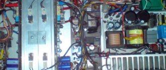
Amplifier AIYIMA A-07 (TPA3255) class D, or “big brother”.
It is long overdue to purchase several inexpensive amplifiers to connect a multi-way speaker system through a digital crossover. For three years, the Breeze Audio TPA3116 MINI amplifier served me faithfully at my dacha and I was inclined to buy a few more of the same ones, but then I came across reviews of several amplifiers based on the new generation of TPA325x chips. The choice fell on AIYIMA amplifiers, but the width of the AIYIMA A-04 = 88mm, and the AIYIMA A-07 = 100mm - the same as my Topping D10 DAC, and everything was decided in favor of the A-07. The main difference between the “big brother” is the TPA3255 chip with power supply up to 50V and twice as much power as the TPA3251. Plus, there is an additional 3.5mm mini-jack AUX input, when a mini-jack plug is connected to it, the RCA input is disabled. Appearance (under the spoiler)
So, since the Chinese are great masters when it comes to manufacturing fake NE5532 operational amplifiers, I prepared my favorite (in terms of sound) AD823 ahead of time to replace them in the preliminary stage of the TPA3255 chip.After receiving it in the mail, we unpack it and turn on the amplifier “kosher”. We connect the GOPHERT CPS-3205E power supply to my old know-how for digital PWM and class D amplifiers - the “snowflake” booster filter, and from there comes the power supply for the amplifier:
Connecting such a booster filter directly to the power input of the amplifier allows, without changing the “native” electrolytic capacitors of the output stage to more capacitive ones, to provide it with a stable voltage at high-speed peak loads, for example, the impact of a bass drum at high volume.
The amplifier was connected to an Optonica CP5000 speaker with a resistance of 8 Ohms (LF - 12″, MF - 2″ dome, HF - ribbon, acoustic design - closed box):
An hour of listening to painfully familiar test tracks
- both the smeared bass and muffled mid-high frequencies increase suspicions about the installation of fake op-amps.
Well, let’s disassemble the amplifier housing and carefully study it:
Unlike AIYIMA A-04, the manufacturer saved two LEDs on the backlight of the volume control:
As expected, the standard NE5532 op-amps turned out to be fake even in appearance: the Texas Instruments logo is crooked, the letters spread out like blots...
Silicone thermal paste on the radiator is:
Electrolytic capacitors of 1000 μF/50V are installed in the output stage of the amplifier. Yes, if it weren’t for the booster filter, then this capacity would not only be enough for 260 Watts of maximum power, but also for 10 Watts.
Op amp - replaced with AD823:
The amplifier has been given a light mod - 0.22 µF film capacitors are used to shunt 10 µF electrolytes, through which the audio signal passes:
We put the “guts” back into the case again, connect the DAC and power.
Now everything has fallen into place: clearly accentuated bass, crystal midrange frequencies and airy highs together form a magical fusion of purity and analyticity with musicality and involvement...
Bottom line: the new generation of TPA325x amplifiers produce decent sound, Hi-Fi level, and raise Class D amplifiers to a new level of quality.
Menu
Most modern integrated op-amps are designed using a direct amplification circuit with differential inputs and are designed for symmetrical bipolar or unipolar power supply. In addition to two inputs, an output and power pins, the op-amp may also have pins for balancing, correction, programming (setting certain parameters by the value of the control current), etc.
Ideally, an op-amp should have infinite voltage gain, infinitely large input and infinitely small output impedance, infinitely large output amplitude, infinitely large range of amplified frequencies, and no noise. The parameters of the op-amp should not depend on external factors, supply voltage and temperature. If these conditions are met, the transfer characteristic of the op-amp covered by negative feedback (NFB) exactly corresponds to the transfer characteristic of the NFC circuit and does not depend on the parameters of the amplifier itself.
Real op-amps have characteristics that differ from ideal ones, which is the reason for their classification by areas and features of application. A real op-amp is a compromise of various requirements with achieving the best properties in one or more parameters, which may be minimizing the offset voltage and input currents, achieving the maximum amplified frequency band and slew rate of the output voltage, reducing current consumption and supply voltage, etc. Op-amp parameters can be divided into several groups - input, output, amplifier, frequency, energy, noise, etc. [].
Along with the operational parameters that determine the nominal operating temperature of the op-amp, the parameters of the input and output circuits and the requirements for power supplies, the maximum permissible (Absolute Maximum Ratings, AMR) values of a number of parameters are very important, exceeding which can lead to failure of the microcircuit. Below is the current classification of op amps according to the combination of various parameters, reflecting their preferred use in a particular class of devices.
Operational amplifiers are also produced, the parameters of which are specially optimized for use in equipment for a specific purpose - medical, automotive, audio devices, etc. Note that the parameters of the op-amp are largely determined by their circuit design and the semiconductor technology used - bipolar transistors (bipolar) , field-effect transistors with pn
-junction (JFET), complementary MOS structures (CMOS) and a combination of complementary pairs of bipolar and field-effect transistors (BICMOS) on one chip.
- Amplifiers for general use: gain - up to 100 dB, offset voltage - more than 1 mV, unity gain frequency - up to 10 MHz.
- Low-power: current consumption - less than 3.5 mA.
- Micropower: current consumption - less than 50 µA.
- Low voltage: supply voltage - less than 3 V.
- Precision: gain - more than 100 dB, offset voltage - less than 1 mV.
- High-speed: unity gain frequency - more than 50 MHz.
- Low noise: noise voltage - less than 10 nV/√Hz.
- Powerful: output current - more than 100 mA.
- With output/input voltage close to supply voltage.
This division, for obvious reasons, is not strict: an op-amp can be simultaneously low-voltage, high-speed, low-noise, with an output voltage close to the supply voltage, etc. In addition, op-amps of the same type are produced in different cases, two or three or four amplifiers in one housing (multi-channel), as well as in versions intended for use in a certain class of devices: for general use (C), for industrial use (I, E) and for special, read - military use (M). They differ in a number of parameters, in particular in the operating temperature range:
- C – 0…+70 °C;
- I— -40…+85 °C;
- E— -40…+ 125 °C;
- M— -55…+ 125 °C.
We also note that in the development of modern operational amplifiers, as well as other integrated circuits, there is a tendency to reduce dimensions and increasingly use surface-mount packages. The previously widespread DIP and TSSOP packages are being replaced by much smaller SOT-23, DFN, QFN, etc.
Devices based on operational amplifiers can be roughly divided into two classes: linear - various amplifiers themselves, including measuring, analog computing circuits, impedance converters, active filters, etc., and nonlinear - analog comparators, voltage multipliers, logarithmic amplifiers, precision rectifiers, signal generators, etc. Moreover, depending on the class of devices and the specific task, certain groups of parameters mentioned at the beginning of the article will be decisive when choosing the type of microcircuit.
In any case, the maximum (minimum) possible values of voltage and current operating in the device being developed should not exceed the limits of the corresponding parameters of the operational amplifier used. This is, first of all, the supply voltage Vcc
, as well as common-mode
Vicm
and differential
Vid
input voltages.
As a rule, modern op-amps have built-in protection against exceeding the maximum value of the output current, and therefore the documentation provides the minimum permissible value of load resistance RL
and the short circuit current of the output to the common power wire
Io
.
Under extreme operating conditions, the operating temperature range of the Toper
, the maximum junction temperature
Tj
, exceeding which in long-term operating modes is not allowed in principle, since in this case the semiconductor
p-n
junction loses its properties, and the thermal resistance of the junction - the environment
Rthja
, measured in °C/W and characterizing the degree of heat transfer from the semiconductor chip crystal into the environment.
During the installation and operation of semiconductor devices, the problem of protecting ICs from electrostatic voltage (Electrostatic Discharge, ESD) arises. If the op-amp has an internal ESD protection circuit, its maximum permissible value is normalized in various configurations, usually within 2 kV.
In the class of linear devices, the most common and in demand are various large-scale amplifiers of direct and alternating current with a relatively small (single to tens) voltage gain. All of them are built on the basis of the standard diagram shown in Fig. 1.
Rice. 1. Typical op-amp scale amplifier circuit
Depending on the choice of external elements and the method of connecting the input signal, the amplifier can be a non-inverting, inverting, differential or buffer follower. In the latter case (V1 - common wire, V2 = Uin
,
ZG
and Z2 are absent, Z1 =
ZF
= 0) the input resistance is determined solely by the parameters of the operational amplifier itself.
Let's look at this using the example of the widely used four-channel op-amp LM2902, made using bipolar technology, and the TS27M4, a CMOS op-amp specifically designed for use in circuits with high input impedance. With other relatively similar parameters given in the table, the typical value of the input current Iib
, which determines the input resistance of the amplifier, is 20 nA for the LM2902 op-amp and only 1 pA for the TS27M4. At the same time, it should be noted that the spread of input current values and its temperature dependence for op-amps made using CMOS technology is usually noticeably greater than for similar op-amps based on bipolar transistors.
Table.
Basic parameters of STMicroelectronics operational amplifiers
| Type | Frame | Temperature range | Supply voltage (peak-to-peak) Vcc, V | Current consumption per channel Icc, mA | Output current Icc, mA | Input current Iib, pA | Bias voltage Vio, µV | Temperature drift of bias voltage ΔVio, µV/°С | Gain Av, dB | Common mode rejection ratio CMR, dB | Supply voltage instability suppression ratio SMR, dB | Common mode input voltage Vin, V | Unity gain frequency. Fu, MHz | Slew rate of output voltage SR, V/µs | Spectral noise density en, nV/√Hz | Note | ||
| min | max | max | max | type. | type. | type. | type. | type. | type. | min | max | type. | type. | type. | ||||
| LM2902/4 | DIP, SO, TSSOP, QFN | E | 3 | 33 | 0,35 | 40 | 20000 | 2000 | 7 | 100 | 80 | 110 | -Vcc-0.3 | +Vcc-1 | 1,3 | 4 | 40 | Standard bipolar |
| TS27M2/4* | DIP, SO, TSSOP | E | 3 | 18 | 0,15 | 30 | 0,001 | 1000 | 2 | 94 | 80 | 80 | -Vcc-0.3 | +Vcc | 1,0 | 0,6 | 38 | Standard CMOS |
| TS512/4 | DIP, SO | I, E | 6 | 36 | 0,50 | 24 | 50000 | 500 | 2 | 100 | 90 | — | -Vcc | +Vcc | 3 | 1,5 | 10 | Precision bipolar |
| TSV731/2/4 | MiniSO, DFN, QFN, TSSOP | E | 1,5 | 5,5 | 0,06 | 10 | 0,001 | 50 | 0,5 | 105 | 94 | 90 | -Vcc-0.2 | +Vcc+0.2 | 0,9 | 0 | 35 | Precision CMOS |
| TSZ121/2/4 | SOT23, DFN, QFN, MiniSO | E | 1,8 | 5,5 | 0,028 | 8 | 0,5 | 1 | 0,01 | 135 | 122 | — | -Vcc-0.2 | +Vcc+0.2 | 0,3 | 0,2 | 40 | Ultra-precision Zero Drift |
| TS971/2/4 | SOT23,SO,DFN | E | 2,7 | 10 | 2 | 100 | 200 | 1000 | 5 | 80 | 85 | 70 | -Vcc-0.3 | +Vcc+0.3 | 12 | 4 | 4 | Ultra-low noise and distortion |
| TSX921 | SOT23 | E | 4 | 16 | 3 | 21 | 0,01 | 5000** | 2 | 110 | 80 | — | -Vcc-0.2 | +Vcc+0.2 | 9 | 17 | 15 | CMOS RRIO |
| TSX9291 | SOT23 | E | 4 | 16 | 2,9 | 21 | 0,01 | 5000** | 2 | 110 | 80 | — | -Vcc-0.2 | +Vcc+0.2 | 15 | 27 | 15 | Same, uncorrected |
| TSH81/2/4 | SOT23,SO,TSSOP | I | 4,4 | 12 | 8,2 | 55 | 6000 | 1100 | 3 | 84 | 97 | 75 | -Vcc | +Vcc-1 | 65 | 105 | 11 | VFA, RRO, THD = 0.1% |
| TSH350 | SOT23, SO | I | 4,5 | 5,5 | 4,1 | 200 | 12/1*** | 1000 | 0,9 | 270**** | 60 | 80 | -Vcc+1.5 | +Vcc-1.5 | 550 | 940 | 1,5 | CFA, THD = 0.1% |
| TSC101/A/B/C | SOT23 | E | 4 | 24 | 0,3 | 26 | 5000 | 700 | 3 | 26/34/40 | 105 | 105 | -0,3 | 60 | 0,5 | 0,9 | — | Current measuring |
| TSC103 | SO, TSSOP | E | 2,7 | 5,5 | 0,3 | 26 | 10000 | 1000** | 5 | 26-40 reg. | 105 | 95 | 2,9 | 70 | 0,7 | 0,6 | 40 | Same with low voltage power supply |
| TS881/2/4 | MiniSO, DFN, QFN, TSSOP | E | 1,1 | 5,5 | 0,0003 | 1,5 | 0,001 | 1000 | 3 | — | 78 | 80 | -Vcc-0.2 | +Vcc+0.2 | — | 5,0***** | — | RRI micropower comparator |
| TS331/2/4 | MiniSO, DFN, QFN, TSSOP | E | 1,6 | 5,5 | 0,022 | 22 | 25 | 500 | 4,5 | — | 75 | 79 | -Vcc-0.3 | +Vcc+0.3 | — | 0,21***** | — | RRI comparator |
| TS3011 | SOT23,SC70 | E | 2,2 | 5,5 | 0,5 | 62 | 0,001 | 400 | 10 | — | 75 | 79 | -Vcc-0.3 | +Vcc+0.3 | — | 0 01***** | — | RRI speed comparator |
Notes.
* Available in three modifications, differing in current consumption and frequency parameters. ** Maximum value. *** Non-inverting/inverting, µA. **** Transimpedance, kOhm. ***** Switching time, µs.
When it is necessary to isolate and amplify a weak signal against a background of strong interference, differential (difference) amplifiers are used (V1, V2 - input signal, ZG
= Z1,
ZF
= Z2).
In an ideal operational amplifier, when these conditions are met, interference creates common-mode signals of equal magnitude at the op-amp inputs, which are successfully suppressed. In real conditions, the choice of op-amp for differential amplifiers requires taking into account several parameters, namely the value of the bias voltage Vio
, its temperature drift Δ
Vio
, common mode rejection ratios (Common Mode Rejection Ratio, CMR) and weakening the influence of the power supply (Supply Voltage Rejection Ratio, SVR ). As an example, let's consider the corresponding parameters for the four-channel op-amp TS514, positioned by the company as a precision version of the above-mentioned op-amp LM2902. Obviously, the use of the TS514 op amp in circuits where common mode rejection is required will be more effective than using standard operational amplifiers.
For strain gauge measurements, to ensure high accuracy, the op-amp must effectively suppress common-mode interference and, in addition, have a high input impedance necessary to match the amplifier with high-impedance strain gauges. In this case, precision field-effect transistor amplifiers are used, for example TSV711/2/4 and TSV731/2/4 (the last digit in the designation corresponds to the number of amplifiers in one package), made using CMOS technology, with a typical input current and bias voltage of 1 pA and 50 µV respectively. It should be borne in mind that the table shows the average parameters of the op-amp, while the proprietary technical documentation, as a rule, indicates in detail the conditions for their determination (supply voltage, temperature, input signals, load resistance, etc.).
The latest STMicroelectronics TSZ121/2/4 operational amplifiers with input and output voltages close to the RRIO (Rail to Rail Input/Output) supply voltage, with automatic zero drift compensation thanks to a very low offset voltage of 1 μV and its temperature drift of 10 nV/° C are called “zero drift amplifiers”. These amplifiers belong to the micro-power group (current consumption - 28 μA) and differ from similar products from other manufacturers in a large range of amplified frequencies (unity gain frequency Fu
= 300 kHz). In Fig. Figure 2 shows graphs of the distribution of bias voltage values of the TSZ121/2/4 op-amp and the dependence of the bias voltage on temperature at a supply voltage of 5 V and a common-mode input voltage of 2.5 V.
Rice. Fig. 2. Distribution of bias voltage values (a) and dependence of bias voltage on temperature (b) TSZ121/2/4 op-amp with a supply voltage of 5 V and a common-mode input voltage of 2.5 V
Consider a situation where minimizing offset voltage can be critical. It is required to design a scale amplifier with a gain of K = 10 to drive the signal to the input of a 12-bit ADC with a maximum input voltage of 4 V. The ADC resolution is 4/212 ≈ 1 mV. If you use the previously discussed precision op-amp TSV7344 with the maximum offset voltage Vio
= 500 µV, the error due to the zero shift will be 5 mV, or more than five LSB units of the ADC, which is completely unacceptable.
At the same time, the use of a TSZ121/2/4 op-amp with a maximum value of Vio
= 5 µV in this amplifier gives a zero shift of no more than 50 µV, which is significantly less than the resolution of the ADC.
When developing amplifiers for weak signals, as well as amplifiers for audio equipment, the noise and dynamic parameters of the op amp become significant - en
, spectral density of the noise voltage referred to the input, measured in nV/√Hz;
total harmonic distortion (Total Harmonic Distortion, THD), measured as a percentage; output voltage slew rate (Slue Rate, SR) - V/µs and unity gain frequency Fu
. (The product of the gain and the bandwidth is also used - Gain Bandwidth Product (GBP)). The last two parameters are decisive for high-frequency amplifiers, the choice of op-amps for which will be discussed in detail below.
The optimal parameters for constructing pre-stage amplifiers for audio equipment are combined with the TS971/2/4 operational amplifier, which is characterized by very low noise levels ( en
= 4 nV/√Hz) and nonlinear distortion (THD = 0.003%). The dependence of the spectral noise density and nonlinear distortion factor on frequency for the TS971/2/4 op-amp at a supply voltage of 5 V is shown in Fig. 3.
Rice. Fig. 3. Dependence of the spectral noise density (a) and nonlinear distortion factor on frequency (b) of the TS971/2/4 op-amp at a supply voltage of 5 V
The stability of operation of circuits based on operational amplifiers with negative feedback and, in particular, the absence of parasitic self-excitation in a wide range of frequencies and gains up to unity is usually ensured by a full frequency response circuit built into the op-amp with a roll-off of 20 dB per decade. In this case, the product of the gain and the bandwidth of the GBP amplifier will be a constant value, as a result of which, at high gain factors, the range of amplified frequencies inevitably narrows. You can expand the frequency band of an op-amp amplifier at high gains by using operational amplifiers with external correction, as shown in Fig. 4.
Rice. 4. Amplitude-frequency characteristics of the corrected and uncorrected operational amplifier
STMicroelectronics' latest designs, the TSX5, TSX6 and TSX9 op amp families, include both corrected and uncorrected op amps designed for use in a wide range of devices operating in the frequency range up to 20 MHz. The adjusted TSX921 op amp with Railto-Rail input and output features low noise and harmonic distortion in the 10 MHz frequency band. Its uncorrected version of the TSX9291 op amp operates stably with gains greater than +2 at frequencies up to 15 MHz.
High-speed operational amplifiers with specific parameters are required for amplification and processing of high-definition video signals, as well as for high-speed communication lines, etc. The calculation shows that if a television video signal amplifier with a resolution of 640×480 and a frame frequency of 50 Hz requires an output voltage slew rate and a unity gain frequency of 105 V/μs and 25 MHz, respectively, then with a resolution of 1600×1200 and a frame frequency of 85 Hz these parameters are already 950 V/µs and 240 MHz.
Recently, two directions have emerged in the circuit design of high-speed op-amps. The first of them is operational amplifiers with voltage feedback (Voltage Feedback Amplifier, VFA), built according to the traditional structural diagram shown in Fig. 5a. It includes a differential input amplifier that has a huge input impedance and, accordingly, low input currents for both the non-inverting (+) and inverting (-) inputs. The main transfer parameter of this op-amp is the voltage gain:
where Vo
- output voltage;
Vd
is the differential input voltage.
Rice. 5. Block diagrams of operational amplifiers: a) with voltage feedback VFA; b) with current feedback CFA
The second direction in the circuit design of high-speed op-amps is the current feedback amplifier (Current Feedback Amplifier, CFA) []. The block diagram of the CFA op-amp is shown in Fig. 5b and consists of buffer amplifier 1 with unity gain and output current In
with a large input and small output resistance, connected between the non-inverting and inverting inputs, and a “current → voltage” converter with a transfer coefficient
Z = Vo/In
, which has the dimension of resistance and is called transimpedance, and therefore such op-amps are called transimpedance.
When switching on transimpedance op-amps with negative feedback according to a non-inverting amplifier circuit (in Fig. 1: V1 - common wire, V2 = Uвx
;
Z1 = 0; Z2 is missing), an error current In
proportional to the input voltage at the non-inverting input flows through the inverting input of the op-amp.
Through the feedback resistor ZF
, connecting the amplifier output and the inverting input, the error current is compensated so that the resulting current through the inverting input tends to zero.
Thus, in transimpedance op-amps, as well as in conventional ones, negative feedback compensates for the amplifier error: for a conventional op-amp this is the differential voltage between the inputs Vd
, and for a transimpedance it is the error current
In
.
The main difference between CFA amplifiers and VFA amplifiers is that by selecting the ZG
and
ZF
can be obtained as shown in Fig. 6, a very wide band of amplified frequencies, practically independent of the gain. Thus, amplifiers with OOS based on CFA op-amp with the same voltage gain are more broadband than amplifiers based on VFA op-amp.
Rice. 6. Frequency response of amplifiers at different voltage gains at the op-amp: a) VFA; b) CFA
Let's compare the parameters of typical high-speed operational amplifiers STMicroelectronics VFA TSH81/2/4 and CFA TSH350 (table). It can be seen that the TSH350 op-amp meets the requirements for amplifiers for high-definition video signals in terms of the rate of rise of the output voltage and the amplified frequency band and can be successfully used in modern video equipment. Both op amps are optimized for 150 ohm load impedance and feature extremely low noise and harmonic distortion levels.
The widespread use of LED light sources required developers to create efficient power supplies with current output, one of the main elements of which are resistive current sensors. There are two main methods for connecting resistive sensors - in a common wire circuit or in a high-potential circuit. In the first case, the sensor is connected between the load and the negative terminal of the power source, in the second - between the positive terminal of the power source and the load. Both methods have their advantages and disadvantages. The advantage of the first is the ability to use conventional precision op-amps to amplify the sensor signal, however, due to the fact that the inclusion of the sensor in the circuit of a common “ground” wire causes voltage to appear between the “ground” of the device itself and the common “ground” conductor, significant contributions are made to the measured signal noise, and the measurement accuracy is very low [].
Measurements using the second method meet the requirements of accuracy and safety, but it requires specialized operational amplifiers that are characterized by a large value of the maximum permissible common-mode voltage with a minimum offset voltage and its drift and the ability to operate at a low unipolar supply voltage. The STMicroelectronics op-amp parameters for amplifying current sensor signals are shown in the table. The amplifiers operate without negative feedback and have a fixed gain (for TSC101 - three values for modifications A/B/C, respectively, for TSC103 - adjustable by applying control voltages to special pins SEL1 and SEL2). A typical circuit diagram for switching on a TSC103 op-amp with single-polar power supply is shown in Fig. 7. It should be noted that this amplifier can also operate with a bipolar supply voltage of ±5 V in the common mode input voltage range from -2.1 to +65 V.
Rice. 7. Circuit for measuring current when a resistive sensor is connected to a high-potential circuit using a specialized op-amp TSC103
Another common type of specialized op amp is analog comparator. Essentially, these are high-quality, high-speed operational amplifiers with a logic output made in a push-pull circuit using bipolar or field-effect transistors, or in an open collector (OC) or open drain (OC) circuit. Comparators, as well as conventional op-amps, are divided into ICs for general use, micro- and low-power, high-speed, etc. Most comparators are designed to operate with single-supply power and are easily interfaced with TTL and CMOS digital devices. The main dynamic parameter of the comparator is the switching time - the time interval from the moment the input voltage is applied to the moment when the voltage at the comparator output reaches the opposite logical level. The switching time depends on the differential input voltage and consists of two parts - the delay time and the rise (fall) time of the voltage at the logic output.
It is important to understand the characteristics of comparators compared to conventional op-amps []:
- In circuits with comparators, negative feedback is almost never used due to the inevitable self-excitation of the device.
- The voltage values at the comparator inputs are different.
- The input impedance of the comparator is relatively small and depends on the levels of the input signals.
- The output impedance of the comparator is relatively high and depends on the output voltage levels.
Comparators are widely used in zero detector circuits, various signal generators, analog-to-digital converters, pulse-width modulator circuits, etc. The STMicroelectronics product list includes several dozen comparators of various types, the parameters of some of them are given in the table.
In Fig. Figure 8 shows a diagram of the temperature control device on the TS332 dual comparator. A micro-power three-terminal thermal sensor STLM20 manufactured by STMicroelectronics is used as a temperature-sensitive element. Resistors set the parameters of the temperature “window”, the outputs of the comparators with an open collector are connected according to the “wiring OR” circuit, the output voltage is supplied to the heater control circuit.
The wide range and low cost of integrated operational amplifiers and comparators from STMicroelectronics make them very attractive for developers of electronic devices. More detailed technical information can be found on the website [].
Rice. 8. Temperature control circuit on a dual comparator TS332
Literature
- Volovich G.I. Circuitry of analog and analog-digital electronic devices. M.: “Dodeka-XXI”, 2005.
- Carter B., Mancini R. Operational amplifiers for everyone. M.: “Dodeka-XXI”, 2011.
- Shtrapenin G.L. High-speed operational amplifiers from National Semiconductor // Chip News - Engineering microelectronics. 2003. No. 10.
- Black B. Current sensor amplifiers for various applications // Electronic components. 2011. No. 2.
- www.st.com