I have already written a similar article about the buck topology, that is, about a step-down converter, today the story will be about how to design a boost voltage converter controlled not by an analog PWM controller, but by a DSP/MK. The prototype will be assembled based on my “development kit” with an STM32F334R8T6 on board and an isolated half-bridge driver.
Introduction
At the beginning, I would like to note one important point - although the article says that control occurs using a microcontroller, this does not mean that the calculation of the power part will be any different from the calculation of a converter with an analog PWM controller.
That is, you can safely use the calculation method from this article when calculating the power section for any boost conveter. In the real world, there are many problems that cannot be solved using standard analog PWM controllers. My favorite example is a voltage converter with an MPPT algorithm. As soon as our task goes beyond the “standard” and some additional control algorithm or operating logic appears, a situation arises in which the use of DSP simplifies the solution of the problem and at the same time makes it cheaper, and most importantly, allows us to solve it in principle.
It’s worth talking a little about the tasks where you will find the boost topology. The topology itself is known to many and many have probably already implemented it when you had, for example, to receive 5V from 1 cell of a li-ion battery - you used a low-power dc/dc boost converter. Such low-power converters are often used in digital electronics, IoT, automation, self-powered devices and other applications.
The second, not entirely obvious, but extremely important application is PFC or power factor corrector. Most PFCs are just a simple boost converter that works using a special algorithm, but in the end it rectifies and boosts the input 85...265VAC to +400VDC. In the future, we will further examine this with an example.
Another frequently encountered option is powerful dc/dc boost converters, for example, network inverters for solar panels with MPPT, which are both the most expensive and most in demand, mainly used in solar power plants with capacities from 5 to 1500 kW. Such converters are built in 2 stages, where the 1st stage is a multiphase dc/dc boost (also Googled as interleaved), which usually receives a constant voltage of 200...600VDC at the input and increases it to a stable 800VDC. Next, an alternating voltage is generated using a conventional dc/ac inverter. Such converters are precisely built on the basis of DSP, and their block diagram looks like this:
I hope you understand why this topology is important for power electronics developers, as well as why it is important to learn how to develop boost converters with DSP/MC-based control. Now with a clear motivation, you can move on to studying topology.
Using the transceiver
You can assemble a step-down voltage converter with your own hands using a step-down voltage transformer. In this case, three amplifiers will be needed. One of them is installed directly behind the inductor. The other two are located behind the transformer. For successful operation of the device, one filter will be enough. The transceiver is connected to the converter via a choke.
To increase current conductivity, you can use a zener diode. A frequency regulator must be installed if the coil is available at 50 A. In other cases there is no need to share the load. The filter will ensure safe operation of the device.
Chapter 1 - Operating principle of the boost topology converter
The boost converter is identical in principle to the buck converter, because in both cases there are two stages of work. At the 1st stage, energy is accumulated in the inductor while the load is powered by the output capacitor. At the 2nd stage, energy is transferred from the inductor to the load and at the same time the output capacitor is charged, which will provide energy to the load while the inductor is “recharging”. Of course, in order to still get a boost converter, circuit changes are necessary, let's look at the circuit diagram of the boost converter:
At first glance, it may seem to you that the topology is not similar to buck, but if you look closely, it will become clear that they are twins. Later you will see this more clearly, but for now let’s look at the stages of operation of the boost converter.
- Charge accumulation stage.
When the converter is turned on, the output capacitance C2 is at potential Vin, because current passes through inductor L1 and diode VD1. The control device (PWM controller or DSP) begins to generate a PWM signal and supplies it to the gate of transistor VT1. When transistor VT1 opens, the circuit is closed, inductance L1 is connected to the power source and begins to accumulate energy. No current flows through VD1, because The potential at the cathode is higher (about Vin) than the potential at the anode (GND potential, about 0V). - Inductance discharge stage.
Now the PWM signal changes its value from 1 to 0 and transistor VT1 closes. At this moment, inductor L1 seeks to maintain the current value by increasing the potential. At the inductor input, the potential is still the same Vin, and therefore the potential increases at the point “choke-drain VT1-anode VD1”. When the potential at this point becomes greater than the potential at the cathode VD1, current will begin to flow through VD1 into the load and in parallel charge the output capacitance C2. At this stage, the circuit is also closed, but not through VT1, but through the “L1-VD1-C2-load” path:
Then these stages simply alternate and the converter works.
For those who don’t understand anything, I’ll explain why the tension increases. At the moment when VT1 closes, the throttle begins to discharge and at the moment of this “discharge” the voltage on it tends to infinity. Yes, this is in an ideal system, but in real life the voltage will be limited by the load resistance, which is connected in series with the inductor and diode, and also, if there is control, also by feedback. Here it is also worth adding on the stage of energy accumulation. At the moment of switching on, there is practically no stored energy in the output capacitor C2, but after the first stage of discharge it is charged and the potential on it is equal to Vout, which means that at subsequent stages of energy accumulation this capacitor C2 will provide the load with energy, as a result there will be no interruptions in the load for receiving energy. It follows from this that C2 must have such a capacity that the stored energy is enough to power the load for the duration of the transistor opening (ton). In accordance with what was described above, starting from the 2nd round of repetition of stages, the charge accumulation stage looks like this:
As you can see, there are two closed circuits. The “red” circuit is closed through VT1 and the inductor is charged, and the “green” circuit is closed through the load. “Mixing” of processes/energy in this case does not occur due to the presence of the VD1 diode, because at any given time, the potential at the cathode VD1 will be higher than the potential at the anode.
Now let's figure out what is happening with the voltage, what connection the output voltage has with the voltage at the input of the converter. As in the case of a buck converter, our boost has a linear dependence of the output voltage on the input, and the transmission coefficient is equal to the duty cycle:
As you can see, the relationship is simple and clear; you can adjust the output voltage accordingly simply by changing the duty cycle of our PWM signal. The algorithm also follows from the regulation formula:
- To increase
the output voltage, you need to
increase
the duty cycle; - To reduce
the output voltage, it is necessary
to reduce
the duty cycle.
Now we understand the operating principle of the boost converter and the logic for controlling the output voltage.
To consolidate our knowledge, let’s analyze a couple of experiments on an oscilloscope and look at these dependencies in practice. For clarity, let’s take a stabilized 10V voltage source, for example, a laboratory power supply, and apply a PWM signal to transistor VT1, the duty cycle of which will be changed during the experiment. The oscilloscope probes are connected to the following points in the circuit:
- Experience No. 1.
The input voltage (Vin) is 12V, the duty cycle of the PWM signal is 0.75: - Experience No. 2.
The input voltage (Vin) is 12V, the duty cycle of the PWM signal is 0.5: - Experience No. 3.
The input voltage (Vin) is 12V, the duty cycle of the PWM signal is 0.25:
Now we have verified in practice that the output voltage depends linearly on the duty cycle, and therefore we can build a control system (CS) that will monitor the output voltage using an ADC and, depending on the measured value, reduce or increase it (duty).
Double resistor devices
A double resistor converter is used much less frequently than other device models. This is due to sudden frequency jumps. For such a converter, you need to use downward thyristors. To reduce the amplitude of interference, first install a transformer, and only then a coil.
Filters for the converter can be selected in a mesh modification. Some frequency control devices use regulators. In addition, an indication system must be installed for the inverter. Terminal blocks are fixed at the transformer output.
Chapter 2 - Boost Converter Design Limitations
As you understand, there is no ideal topology, otherwise there wouldn’t be so many of them and everyone would use only it, for example, a full bridge. In this case, boost converters also have a number of features that impose restrictions on the use of this topology:
- The output voltage should not exceed the input voltage by more than 3...4 times.
Experts will probably come running here and tell you how they increased the boost voltage from +5V to as much as +180V in a clock on IN-12 using MC34063! This is, of course, wonderful, but let's estimate the duty cycle for this case, in order to raise the voltage from 5V to 180V, you need to make the converter work at a coefficient of about
0,972
(!). I think there is no need to tell you that this is a bad idea, that at high frequencies the transient process when switching transistors will have a comparable duration, and maybe even longer.Also, with such a fill factor, it turns out that the transistor is almost always open, which means current flows through it and we get the maximum possible value of static losses, and therefore low efficiency.
What does this actually lead to... at low power (the same case with the mc34063), unstable operation, low reliability, current ripple and low efficiency are guaranteed, combined with increased heating of the power elements. At high power - boom.
For example, pay attention to PFC, they all work with a ratio of maximum 1:4, namely the same universal input 85...265VAC or a voltage stabilizer with their 90...310VAC. Also, as an example, we can consider network inverters with MPPT, where at an output of 800V, 200...600VDC is supplied to the input, that is, a ratio of 1:4;
- Transistor voltage.
This limitation is closely related to the thesis about the ratio above and here’s why... Transistor VT1 must have a drain-source voltage equal to the minimum output voltage, and in real devices it must also have a margin of at least 20% for ripple. High-voltage switches have a high channel resistance, and with a large voltage ratio, the input current will be very large, which will lead to large losses in the transistor; - Diode voltage.
If you look closely at the converter circuit, it will become clear that a voltage equal to the output voltage is applied to the diode VD1, that is, if you have an output of 400V, then the diode must withstand this 400V.In this regard, this topology has an interesting “plus”, because Since the diode is high-voltage and the current flows in it is several times lower than the current through the transistor, then in many solutions the use of a Schottky diode or SiC diode will result in lower losses than the use of synchronous topology (half-bridge on transistors). This applies to solutions with an output of 200V or more, and the synchronous version of the topology is mainly relevant only up to a voltage of about 100V;
- Capacitor voltage.
It seems like an obvious point, but just in case, I’ll clarify - the output capacitor must withstand a voltage equal to the output voltage, which in many tasks where boost is used can be 400, 800 or even 1500VDC.
From what was written above, I think it is quite obvious that it is reasonable to use a boost converter when you need to increase the voltage by a maximum of 3...4 times and no galvanic isolation is needed; in other cases you need to look towards push-pull or full bridge topologies. The power for boost converters, in principle, has no upper limit; there are also PFCs for tens of kilowatts and inverters for solar power plants for megawatts, which are built on this topology.
Prologue.
I have two multimeters, and both have the same drawback - they are powered by a 9-volt Krona battery.
I always tried to have a fresh 9-volt battery in stock, but for some reason, when it was necessary to measure something with an accuracy higher than that of a pointer instrument, the Krona turned out to be either inoperative or only lasted for a few hours of operation.
The last time, I had to alternately recharge two crowns from the power supply in order to make the necessary measurements, although 12.2012 was written on the crowns. In general, patience came to an end, and I got to work.
Chapter 3 - Calculation of the power part of the converter
It's time to calculate the main power elements for assembling the prototype. As a power source, I will use a laboratory power supply with a 12V output, because... if someone wants to repeat it, but there is no LBP, then you can use the usual Chinese Mean Well at 12V 5A. Today, the visual load will be a 36V incandescent lamp with a power of 60 W. I specifically selected the source and load so that the model could be assembled in any village, at the same time cheaply and maintain a 1:3 ratio. In total we have the following input data:
- Input voltage: 12V
- Output voltage: 36V
- Rated power: 60W
- Conversion frequency: 100 kHz
Calculation and manufacture of the throttle
I'll start with the most interesting and important, because... It is with the calculation of power inductance that developers usually have problems. I should immediately note that I will calculate the inductance value for the continuous current mode
(CCM).
First, let's find the maximum duty cycle value at which our converter will operate. This value will be set by the PWM controller at the minimum input voltage. For example, I plan to power the converter from a stabilized power supply, then Vmin = Vnom
.
If you choose, for example, a lead battery as a power source, then the voltage range is 10.2...14.2V and in this case for calculations you need to take the value 10.2V, because this will achieve the maximum fill factor. I will take the value equal to 12V as a minimum
. The calculation formula itself is simple and looks like this:
Now we need to calculate the current ripple in the inductor. Those who read my article about the buck converter probably remembered that we choose this value ourselves and usually it is set from 20 to 50%, but I will take a range of 30% and now we will find the current value itself:
Now let's calculate the minimum inductance value that is required to remain in the continuous current mode:
To make the throttle, I will take the R26/14/11 throttle (R is the ring, and the numbers are the dimensions) from Kool Mu material with a permeability of 60, you can download the documentation for it and buy it here - Lapkos.
Now let's find out how many turns we need to get this minimum inductance:
This is the minimum number of turns at which the converter will remain in continuous current mode with a minimum input voltage of 12V. To be safe, let's throw on a few more turns just to be sure and wind 3 more turns, that is, 29 turns
. Let's find out what inductance we will ultimately get with this number of turns:
We have received a new (final) inductance value and the number of turns, let's check whether we have exceeded the induction limit for this core:
The core is made of Kool Mu material for which the induction limit is 0.5 Tesla. As you can see, with this core we have a five-fold reserve. N - reliability! From this we can indirectly conclude that at a frequency of 100 kHz, about 300 W can be pumped through this core.
Now let's decide on the winding wire. I have a lot of my favorite wire in stock with a diameter of 0.6 mm, which corresponds to a cross-section of one core of 0.283 mm2. The average current in the core will be about 5A, so if we wind it in one core, we will get a current density equal to 5A / 0.283 mm2 = 17.66 A/mm2
, which is too much and there will be excessive heating of the throttle.
There is a lot of space for winding, the core is large, so I will wind it in 2 cores
, which will reduce the current density by 2 times to a value of
8.83 A/mm2
. This will allow you to get overheating relative to the environment within +20 oC.
All parameters of the inductor were determined: dimensions R26/14/11, material Kool Mu, number of turns 29, winding wire with a diameter of 0.6 mm and winding in 2 cores. Let's go reel in:
We wound it, secured the end of the winding, secured the entire winding with tape - ready. It remains to measure the actual value of the inductor inductance:
We got the required value! Now you can safely move on to calculating the output capacitance. The logic is simple in principle - the larger the output capacitance, the lower the ripple. However, it is worth understanding that if the capacitance is taken several orders of magnitude larger than the calculated value, then the time constant will be too large and the control system (CS) will not work correctly, so we will calculate the minimum capacitance value for the capacitor (C2):
At frequencies within 200 kHz, where cheap electrolytes are still installed, I usually multiply this minimum value by 2...3 and set this value. In the current task, I am using a debug power module, and electrolytes are already installed on it, which play the role of an output capacitance in the boost topology, which I will talk about in more detail in the next chapter.
The total capacity of the electrolytes is 3000 μF, which is a lot in this task, because The board was designed for higher powers. With such a large output capacitance, feedback is not easy, but it’s good for experiments.
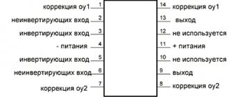
All that remains is to briefly talk about transistors. It's about transistors! I am using a half bridge module and therefore implementing a synchronous boost converter. The modules are equipped with IPP083N10N5AKSA1 transistors with a drain-source voltage of 100V, which gives an almost threefold voltage reserve and therefore covers the task - we pass through the transistor VT1, and the diode VD1 is replaced with a similar transistor and, accordingly, we also pass.
Pulse width modulation
The output parameters are adjusted by controlling the duration of the open and closed states of the key element. The most common principle is pulse width modulation.
The transistor is switched by high-frequency pulses of constant frequency. Opening and closing times are determined by the width of the pulses. The tracking circuit monitors the output voltage by comparing it with a reference. The mismatch signal is sent to the modulator, which regulates the parameters of the control pulses.
Pulse width modulation
In modern designs, all these functions are assigned to a specialized integrated circuit, making the circuit design of switching power supplies with pulse width modulation (PWM) simple and reliable.
Chapter 4 - Code to Control the Converter
Since I will talk about control algorithms in a separate article, today the converter will be controlled by the same program that was used in the article that talked about the buck topology, you can read it here.
In the code chapter you can read in detail about the initialization of HRPWM and ADC, as well as their synchronization. Changes in the code occurred only in one place, namely in the interrupt handler with the ADC - the cutoff threshold changed, because I used a different voltage divider. Well, I corrected the condition so that there was no excessive overshoot:
void ADC1_2_IRQHandler (void) { ADC2->ISR |= ADC_ISR_EOC; adcResult = ADC2->DR; if (adcResult >= 3400) { dutyControl = dutyControl - 10; } else { dutyControl = dutyControl + 10; } SetDutyTimerA(dutyControl); } You will find the original project for TrueSTUDIO at the end of the article in archive form. Now that the principle of operation of the converter has been disassembled, all components have been calculated, and there is a control program, you can begin assembling the layout and testing it for operability and the correctness of the results obtained.
Transformer with open rectifier
It is very easy to assemble such a converter with your own hands. First you need to install the coil with the primary winding. Choose those that can withstand voltages greater than 30 Ohms. The rectifier itself is mounted adjacent to the tetrode.
It is better to choose open resistors. An amplifier cannot be installed in this circuit. If you are building a 60A device, they should be soldered next to the coil. When everything is ready, the terminal blocks are secured.
Chapter 5 — Assembling the layout and testing the converter
Let's proceed to the most interesting and colorful stage, namely, assembling the layout and checking its functionality. At the beginning of the article, I mentioned the relationship between buck and boost topologies, let's look at this now, because on the half-bridge module this is extremely clear. First of all, let's look at the buck converter circuit:
The green frame highlights the components that are installed on the half-bridge power module, as you can see here C1 acts as an input capacitance, and capacitor C2 acts as an output capacitor. Now let's depict the boost converter circuit:
Who is attentive and noticed what has changed? Yes, in principle, nothing has changed, oddly enough, the only difference is that the entrance and exit have changed places. As you can see, the topologies themselves are identical, and this leads to another interesting property - if a synchronous topology is used, then the converter can work as a bidirectional converter!
Example? Easily! Let's imagine a portable device with USB and Li-ion battery. When the USB is connected, the converter operates in buck mode and charges the battery; as soon as the USB cable is disconnected, the converter switches to boost mode and raises from 4.2V to 5V from which the device is powered. Cool! And there are quite a lot of similar tasks where this feature is useful.
I assembled the prototype according to the second circuit, and in it the capacitor C1 is exactly the output capacitance, that is, it is already installed and it is enough to put the inductor that we made and the input capacitance on the module. I used a pair of 4700 µF 25V electrolytic capacitors as input capacitance C2 and ended up with this layout of the power section:
Now we connect the control module and power source to the power part, in this case a laboratory power supply:
Now let’s upload the firmware to the microcontroller, supply power from the laboratory, set the duty cycle to 30,000 out of 45,000, which, according to our formula, will increase the input voltage by 3 times: Vout = 12V / (1 - 0.66) = 12/0.33 = 36.36V . After this we will see that the lamp lights up brightly:
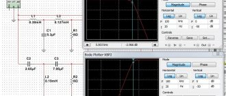
Now we connect the oscilloscope to the same points and see the following result:
As you can see, the device works correctly: the voltage has actually increased 3 times, the input consumption is about 60 W ( yes, I know that the lamp needs 36V “changes”
), the lamp itself consumes a current of 1.61 A. For clarity, I’ll leave a short video in progress:
It remains to find out how much the converter heats up under these conditions.
I assumed that overheating would be minimal, because... everything was calculated correctly, and the components were taken with reserve, so I placed the converter in an environment with a temperature of approximately +10 oC to enhance the contrast of the temperature field. My testing method is simple and consists of three stages:
- I place the converter in an environment with a temperature of +10 oC and wait until it cools down and becomes practically indistinguishable in the thermal imager against the general background;
- I turn on the converter, let it run for 5 minutes and measure the general appearance of the converter and separately the power components;
- I leave the converter running for another 1 hour and measure again to see how much the component temperatures have increased.
After this experiment, it will be possible to draw approximate conclusions about the possibility of operating the converter in long-term modes, as well as understand how much the device overheats relative to the ambient temperature, which will make it possible to predict the behavior of the device at higher ambient temperatures. And so let's get started:
- Measurement No. 1 - the converter was placed in an environment with a temperature of about +10 oC:
Here you can see that the boards have almost completely merged with the environment, which means you can turn on and begin assessing the temperatures of the converter already under rated load.
- Measurement No. 2 - the converter operates at 100% rated load for 5 minutes, ambient temperature is about +10 oC:
After 5 minutes of operation, the picture became more contrasting and both the converter itself and the main heating components were clearly visible. The record holders for overheating are insulated dc/dc for transistor drivers with a temperature of +29 oC, but there is nothing strange here, because the overheating temperature of +20…30 oС is nominal for them, which is reflected in the documentation. The second place is occupied by the throttle, the temperature of which is +28...29 oС, which is more than good, because Often the operating chokes may well reach the bar at +80...100 oC. The radiator temperature is +20...21 oC, and the transistors are only a degree hotter, or maybe less, because Any thermal imager is actually not the most accurate device in the world.
- Measurement No. 3 - the converter operates at 100% rated load for 1 hour, ambient temperature is about +10 oC:
After an hour of operation, the temperatures increased and settled down, I tried to measure again after 3 hours, but the result did not change, or rather the changes were at the level of measurement error, so I did not add this stage. For now, let's look at the temperatures after the converter reaches cruising speed in the nominal mode.
The temperature of the radiator increased by +4 oC, and the transistors “merged” with it, because everything warmed up and the heat flow was evenly distributed. The temperature on the isolated dc/dc increased by +9 oC and they reached the overheating ratings, even the margin remained a couple of degrees. The throttle temperature increased by +3 oC.
Let's summarize... The temperature of the transistors is normal, which means the losses are negligible and the power module itself works correctly, there are no through currents, there are no problems with installing the transistors, by the way, they sit on a ceramic substrate in a drop of MX-4 thermal paste, you don’t need to add a lot of paste - will be worse.
The temperature of the inductor is also normal, which means the inductance was calculated correctly and the core dimensions were also suitable, yes, with a 5-fold margin :)), that is, it does not become saturated and the winding does not overheat with the current value of the current density.
Bonus for the curious
Keep a light bulb in your thermal imager :))
Additional materials:
Articles:
- Maxim Integrated nanoPower Technology: When Low IQ Benefits
- Sleep Control: Improve Battery Efficiency with DC/DC MAX17225 nanoPower
- One choke for the entire system: Maxim multichannel converters with SIMO and nanoPower technologies
- Real-time power measurement using power logger IC
- Extending the runtime of portable electronics with a SIMO-based converter
- SIMO fighters: features of using Maxim SIMO converters
- Selecting a SIMO PMIC Converter for a Handheld Device Project
- Increasing the energy efficiency of portable devices using SIMO PMIC converters
News
- MAX17222 - long life for small things
- MAX38640/1/2/3 – step-down converters of the NanoPower family with ultra-low current consumption
- MAX17270 – NanoPower SIMO PMIC for IoT with ultra-low power consumption
•••
Refinement of the multimeter.
The DT-830B multimeter immediately started working with the upgraded Krona. But the M890C+ tester had to be slightly modified.
The fact is that most modern multimeters have an automatic power-off function. The picture shows part of the multimeter control panel where this function is indicated.
The Auto Power Off circuit works as follows. When the battery is connected, capacitor C10 is charged. When the power is turned on, while capacitor C10 is discharged through resistor R36, the output of comparator IC1 is held at a high potential, which causes transistors VT2 and VT3 to turn on. Through the open transistor VT3, the supply voltage enters the multimeter circuit.
As you can see, for normal operation of the circuit, you need to supply power to C10 even before the main load turns on, which is impossible, since our modernized “Krona”, on the contrary, will turn on only when the load appears.
In general, the whole modification consisted of installing an additional jumper. For her, I chose the place where it was most convenient to do this.
Unfortunately, the designations of the elements on the electrical diagram did not match the designations on the printed circuit board of my multimeter, so I found the points for installing the jumper this way. By dialing, I identified the required output of the switch, and identified the +9V power bus using the 8th leg of the operational amplifier IC1 (L358).
Small details.
It was difficult to purchase just one battery. They are mostly sold either in pairs or in groups of four. However, some kits, for example, “Varta”, come with five batteries in a blister. If you are as lucky as I am, you will be able to share such a set with someone. I bought the battery for only $3.3, while one “Krona” costs from $1 to $3.75. There are, however, also “Crowns” for $0.5, but they are completely stillborn.
March 19, 2012 (15:23) in Power supplies, DIY
Disassembling a nine-volt Krona battery.
To complete this project, I carefully bent the rolled edge of the back of the tin housing.
In the corners I bent the folding using a thin screwdriver.
Using pliers, I smoothed out the deformed edge of the shell.
Removed battery sections.
I drilled a hole with a diameter of 6mm in the back wall and screwed in a standard socket for a 3.5mm Jack so that the built-in battery could later be charged without disassembly.