Nikolay Petrushov
TL494 (Texas Instruments) is probably the most common PWM controller, on the basis of which the bulk of computer power supplies and power parts of various household appliances were created. And even now this microcircuit is quite popular among radio amateurs who are building switching power supplies. The domestic analogue of this microcircuit is M1114EU4 (KR1114EU4). In addition, different foreign companies produce this microcircuit with different names. For example IR3M02 (Sharp), KA7500 (Samsung), MB3759 (Fujitsu). It's all the same chip. Its age is much younger than TL431. It began to be produced by Texas Instruments somewhere in the late 90s - early 2000s. Let's try to figure out together what she is and what kind of “beast” this is? We will consider the TL494 chip (Texas Instruments).
So, first, let's see what's inside.
Manufacturers
The microcircuit in question belongs to the list of the most common and widely used integrated electronic circuits. Its predecessor was the UC38xx series of PWM controllers from Unitrode. In 1999, this company was purchased by Texas Instruments, and since then the development of the line of these controllers began, leading to the creation in the early 2000s. TL494 series chips. In addition to the UPS already mentioned above, they can be found in DC voltage regulators, controlled drives, soft starters - in a word, wherever PWM regulation is used.
Among the companies that cloned this chip are such world-famous brands as Motorola, Inc, International Rectifier, Fairchild Semiconductor, ON Semiconductor. They all provide a detailed description of their products, the so-called TL494CN datasheet.
Documentation
An analysis of descriptions of the type of microcircuit in question from different manufacturers shows the practical identity of its characteristics. The amount of information provided by different companies is almost the same. Moreover, the TL494CN datasheet from brands such as Motorola, Inc and ON Semiconductor replicate each other in their structure, figures, tables and graphs. The presentation of the material by Texas Instruments is somewhat different from them, but upon careful study it becomes clear that they are referring to an identical product.
Status
| TL494CD | TL494CDG4 | TL494CDR | TL494CDRE4 | TL494CDRG3 | TL494CDRG4 | TL494CJ | TL494CN | TL494CNE4 | TL494CNSR | TL494CNSRG4 | TL494CPW | TL494CPWG4 | TL494CPWLE | TL494CPWR | TL494CPWRG4 | TL494ID | TL494IDG4 | TL494IDR | TL494IDRE4 | TL494IDRG4 | TL494IN | TL494INE4 | TL494MJ | TL494MJB | |
| Product Status | In production | In production | In production | In production | Announced | In production | Out of production | In production | In production | In production | In production | In production | In production | Out of production | In production | In production | In production | In production | In production | In production | In production | In production | In production | Out of production | Out of production |
| Availability of samples from the manufacturer | Yes | No | No | No | No | No | No | No | No | No | No | No | No | No | Yes | No | No | No | No | Yes | No | Yes | No | No | No |
Purpose of the TL494CN chip
Traditionally, we will begin our description with the purpose and list of internal devices. It is a fixed-frequency PWM controller intended primarily for UPS applications, containing the following devices:
- sawtooth voltage generator (RPG);
- error amplifiers;
- reference voltage source +5 V;
- “dead time” adjustment circuit;
- output transistor switches for current up to 500 mA;
- scheme for selecting one- or two-stroke operating mode.
Limit parameters
Like any other microcircuit, the TL494CN description must necessarily contain a list of maximum permissible performance characteristics. Let's give them based on data from Motorola, Inc:
- Supply voltage: 42 V.
- Collector voltage of output transistor: 42 V.
- Output transistor collector current: 500 mA.
- Amplifier input voltage range: from - 0.3 V to +42 V.
- Power dissipation (at t<45 °C): 1000 mW.
- Storage temperature range: from -55 to +125 °C.
- Operating ambient temperature range: from 0 to +70 °C.
It should be noted that parameter 7 for the TL494IN chip is somewhat wider: from –25 to +85 °C.
TL494CN: functional diagram
So, the task of this microcircuit is pulse width modulation (PWM, or Pulse Width Modulated (PWM)) of voltage pulses generated inside both regulated and unregulated UPSs. In power supplies of the first type, the range of pulse durations, as a rule, reaches the maximum possible value (~ 48% for each output in push-pull circuits, widely used to power car audio amplifiers).
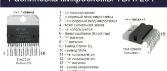
The TL494CN chip has a total of 6 output pins, 4 of them (1, 2, 15, 16) are inputs to internal error amplifiers used to protect the UPS from current and potential overloads. Pin #4 is a 0 to 3V signal input to adjust the duty cycle of the square wave output, and #3 is a comparator output and can be used in several ways. Another 4 (numbers 8, 9, 10, 11) are free collectors and emitters of transistors with a maximum permissible load current of 250 mA (in long-term mode no more than 200 mA). They can be connected in pairs (9 with 10, and 8 with 11) to control powerful field-effect transistors (MOSFET transistors) with a maximum permissible current of 500 mA (no more than 400 mA in continuous mode).
What is the internal structure of the TL494CN? Its diagram is shown in the figure below.
The microcircuit has a built-in reference voltage source (RES) +5 V (No. 14). It is usually used as a reference voltage (with an accuracy of ± 1%), supplied to the inputs of circuits that consume no more than 10 mA, for example, to pin 13 for selecting one- or two-cycle operating modes of the microcircuit: if +5 V is present on it, the second mode is selected , if there is a minus supply voltage on it - the first one.
To adjust the frequency of the ramp voltage generator (RVG), a capacitor and resistor are used, connected to pins 5 and 6, respectively. And, of course, the microcircuit has pins for connecting the plus and minus of the power supply (numbers 12 and 7, respectively) in the range from 7 to 42 V.
The diagram shows that there are a number of other internal devices in the TL494CN. A description in Russian of their functional purpose will be given below as the material is presented.
Datasheets
ProductFolder OrderNow Support &Community Tools &Software TechnicalDocuments TL494SLVS074H – JANUARY 1983 – REVISED MARCH 2022 TL494 Pulse-Width-Modulation Control Circuits1 Features 1 Complete PWM Power-Control CircuitryUncommitted Outputs for 200-mA Sink orSource CurrentOutput Control Selects Single -Ended orPush-Pull OperationInternal Circuitry Prohibits Double Pulse atEither OutputVariable Dead Time Provides Control OverTotal RangeInternal Regulator Provides a Stable 5-VReference Supply With 5% ToleranceCircuit Architecture Allows Easy Synchronization 2 Applications Desktop PCsMicrowave OvensPower Supplies: AC/DC, Isolated,With PFC, > 90 WServer PSUs …
Input pin functions
Just like any other electronic device. the microcircuit in question has its own inputs and outputs. We'll start with the first ones. A list of these TL494CN pins has already been given above. A description in Russian of their functional purpose will be given below with detailed explanations.
Conclusion 1
This is the positive (non-inverting) input of error amplifier 1. If its voltage is lower than the voltage at pin 2, the output of error amplifier 1 will be low. If it is higher than at pin 2, the error amplifier 1 signal will become high. The amplifier's output essentially follows the positive input using pin 2 as the reference. The functions of error amplifiers will be described in more detail below.
Conclusion 2
This is the negative (inverting) input of error amplifier 1. If this pin is higher than pin 1, the output of error amplifier 1 will be low. If the voltage on this pin is lower than the voltage on pin 1, the amplifier output will be high.
Conclusion 15
It works exactly the same as #2. Often the second error amplifier is not used in the TL494CN. The connection circuit in this case contains pin 15 simply connected to 14 (reference voltage +5 V).
Conclusion 16
It works in the same way as No. 1. It is usually attached to the common No. 7 when the second error amplifier is not used. With pin 15 connected to +5V and pin 16 connected to common, the output of the second amplifier is low and therefore has no effect on the operation of the chip.
Conclusion 3
This pin and each internal TL494CN amplifier are coupled together via diodes. If the signal at the output of any of them changes from low to high level, then at No. 3 it also goes high. When the signal at this pin exceeds 3.3 V, the output pulses are turned off (zero duty cycle). When the voltage across it is close to 0 V, the pulse duration is maximum. Between 0 and 3.3 V, the pulse duration is from 50% to 0% (for each of the PWM controller outputs - at pins 9 and 10 in most devices).
If necessary, pin 3 can be used as an input signal or can be used to provide damping for the rate of change of pulse width. If the voltage on it is high (> ~3.5V), there is no way to start the UPS on the PWM controller (there will be no pulses from it).
Conclusion 4
It controls the duty cycle range of output pulses (English Dead-Time Control). If the voltage across it is close to 0 V, the microcircuit will be able to output both the minimum possible and maximum pulse width (which is determined by other input signals). If a voltage of about 1.5V is applied to this pin, the output pulse width will be limited to 50% of its maximum width (or ~25% duty cycle for a push-pull PWM controller mode). If the voltage is high (>~3.5V), there is no way to start the UPS on the TL494CN. Its connection circuit often contains No. 4, connected directly to ground.
- Important to remember! The signal at pins 3 and 4 should be below ~3.3 V. But what happens if it is close to, for example, +5 V? How will the TL494CN behave then? The voltage converter circuit on it will not generate pulses, i.e. there will be no output voltage from the UPS.
Conclusion 5
Serves to connect the timing capacitor Ct, with its second contact connected to ground. Capacitance values are typically between 0.01 µF and 0.1 µF. Changes in the value of this component lead to changes in the frequency of the GPG and the output pulses of the PWM controller. Typically, high quality capacitors with a very low temperature coefficient (with very little change in capacitance with temperature) are used.
Conclusion 6
To connect the drive-setting resistor Rt, with its second contact connected to ground. The values of Rt and Ct determine the frequency of FPG.
- f = 1.1: (Rt x Ct).
Conclusion 7
It connects to the common wire of the device circuit on the PWM controller.
Conclusion 12
It is marked with the letters VCC. It is connected to the “plus” of the TL494CN power supply. Its connection circuit usually contains No. 12, connected to the power supply switch. Many UPSs use this pin to turn the power (and the UPS itself) on and off. If there is +12 V on it and No. 7 is grounded, the GPN and ION microcircuits will work.
Conclusion 13
This is the operating mode input. Its functioning has been described above.
Repair of ATX/AT unit (methodology)
Repair of the ATX/AT unit (methodology) Repair of the ATX/AT unit (methodology)
A typical diagram can be found here: AT and ATX All work with a switching power supply should be carried out by disconnecting it from the ~220V network!!! Control circuit.
Checking the block begins with the control circuit.
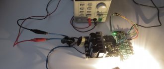
(PWM controller TL494CN) A description of the microcircuit can be found here. To do this, you will need a stabilized 12V power supply. We connect the UPS under test to the circuit as shown in the diagram in Fig. 1 and look at the presence of oscillograms at the corresponding terminals. Take oscilloscope readings relative to the common wire. Fig.1 Checking the functionality of the TL494CN After checking, do not forget to return pin 4 to the circuit!!! High voltage circuit.
To do this, we sequentially check: a fuse, a protective thermistor, coils, a diode bridge, high-voltage electrolytes, power transistors (2SC4242), the primary winding of the transformer, control elements in the base circuit of power transistors.
(see Fig. 2 and Fig. 3) Power transistors usually burn out first.
It is better to replace with similar ones: 2SC4242, 2SC3039, KT8127(A1-B1), KT8108(A1-B1), etc. Elements in the base circuit of power transistors. (check the resistors for open circuits) As a rule, if the diode bridge burns out (the diodes ring short), then high voltage electrolytes fly out from the alternating current entering the circuit. Usually the bridge is RS205 (2A 500V) or worse. Recommended - RS507 (5A 700V) or equivalent. Well, the fuse is always the last one to burn. .52V. Fig.2 Checking the input circuit. If everything is in order, then you can move on to the next point. Checking the operation of power transistors.
In principle, there is no need to check operating modes. If the first two points are passed, then the power supply can be considered 99% serviceable. However, if the power transistors were replaced with other analogs or if you decided to replace bipolar transistors with field-effect ones (for example, KP948A, the pinout is the same), then you need to check how the transistor handles transient processes. To do this, you need to connect the unit under test as shown in Fig. 1 and Fig. 2. Disconnect the oscilloscope from the common wire! Oscillograms on the collector of a power transistor are measured relative to its emitter. (as shown in Fig. 3, the voltage will vary from 0 to 51V) In this case, the process of transition from low to high level should be instantaneous. (or almost instantaneously).
This largely depends on the frequency characteristics of the transistor and damper diodes (in Fig. 3 FR155. analogue of 2D253, 2D254). If the transition process occurs smoothly (there is a slight slope), then most likely within a few minutes the radiator of the power transistors will become very hot. (during normal operation, the radiator should be cold) Fig. 3 Checking the operation of power transistors. Checking the output parameters of the power supply.
After all the above work, it is necessary to check the output voltages of the unit. Voltage instability under dynamic load, intrinsic ripple, etc. You can, at your own peril and risk, plug the unit under test into a working motherboard or assemble the circuit shown in Fig. 4 Fig.4 Simplified power supply load diagram. This circuit is assembled from PEV-10 resistors. Mount the resistors on an aluminum radiator.
(a 20x25x20 channel is very suitable for these purposes) Do not turn on the power supply without a fan! It is also advisable to blow on the resistors. Observe ripples with an oscilloscope directly at the load. (from peak to peak there should be no more than 100 mV, in the worst case 300 mV) In general, it is not recommended to load the power supply with more than 1/2 of the declared power. (for example: if it is indicated that the power supply is 200 Watt, then load no more than 100 Watt) If desired, the load circuit can be complicated: Fig. 4.1 Extreme load of the power supply. Self-generating auxiliary source.
Used to power the TL494CN and the +5Vsb stabilizer (see ATX block diagram) Options for auxiliary sources in inexpensive units: Fig. 5 Option 1 Fig. 6 Option 2 In more expensive power supplies, additional sources are implemented on TOPSwitch series microcircuits.
KA1H0165R KA1H0165RN ...or the second option: .| Part | Value | Part | Value |
| R101 | 100 kOhm | D101 | UF4007 |
| R102 | 500 kOhm | D102 | 1N4937 |
| R103 | 120 Ohm | D103 | 1N4948 |
| R104 | 1.2 kOhm | D201 | Shottoky |
| C101 | 222/630V | C202 | 470mF/10V |
| C103 | 222 uF | R201 | 500 Ohm |
| ZD101 | 12V/0.
| D201 | 20mH |
For a description in Russian, see the website www.compitech.ru here or use the search engine www.av.com Back
Output Pin Functions
They were also listed above for the TL494CN. A description in Russian of their functional purpose will be given below with detailed explanations.
Conclusion 8
This chip has 2 NPN transistors, which are its output switches. This pin is the collector of transistor 1, usually connected to a constant voltage source (12 V). However, in the circuits of some devices it is used as an output, and you can see a square wave on it (as on No. 11).
Conclusion 9
This is the emitter of transistor 1. It drives the UPS power transistor (FET in most cases) in a push-pull circuit, either directly or through an intermediate transistor.
Conclusion 10
This is the emitter of transistor 2. In single-cycle mode, the signal on it is the same as on No. 9. In push-pull mode, the signals on No. 9 and 10 are antiphase, i.e., when the signal level is high at one, then it is low at the other, and vice versa. In most devices, signals from the emitters of the output transistor switches of the microcircuit in question control powerful field-effect transistors, which are turned ON when the voltage at pins 9 and 10 is high (above ~ 3.5 V, but it does not in any way relate to the 3.3 V level at No. No. 3 and 4).
Conclusion 11
This is the collector of transistor 2, usually connected to a constant voltage source (+12 V).
- Note: In devices based on TL494CN, its connection circuit may contain both collectors and emitters of transistors 1 and 2 as outputs of the PWM controller, although the second option is more common. There are, however, options when exactly pins 8 and 11 are outputs. If you find a small transformer in the circuit between the microcircuit and the field-effect transistors, the output signal is most likely taken from them (from the collectors).
Conclusion 14
This is the ION output, also described above.
Scope of application TL494
Among the main areas of application, you should pay attention to the following:
- computers – stationary models;
- microwave ovens and other small household appliances;
- uninterruptible power supplies whose power does not exceed 9 V;
- ultraviolet radiation energy converters;
- power supplies located in an isolated space;
- converters.
Also, many radio amateurs use this chip for training and research.
Principle of operation
How does the TL494CN chip work? We will give a description of how it works based on materials from Motorola, Inc. Pulse width modulation output is achieved by comparing the positive ramp signal from capacitor Ct with either of the two control signals. The NOR logic circuits control the output transistors Q1 and Q2, opening them only when the signal at the clock input (C1) of the flip-flop (see the TL494CN functional diagram) goes low.
Thus, if the input C1 of the trigger is at a logical one level, then the output transistors are closed in both operating modes: single-cycle and push-pull. If there is a clock signal at this input, then in push-pull mode the transistor switches open one by one when the clock pulse cutoff arrives at the trigger. In single-ended mode, a flip-flop is not used and both output switches open synchronously.
This open state (in both modes) is possible only in that part of the GPG period when the sawtooth voltage is greater than the control signals. Thus, an increase or decrease in the value of the control signal causes a corresponding linear increase or decrease in the width of the voltage pulses at the outputs of the microcircuit.
The voltage from pin 4 (dead time control), the inputs of error amplifiers, or the feedback signal input from pin 3 can be used as control signals.
Design features and installation recommendations
The appearance of the device is shown in Figure 2. The device is housed in an ATX-400W power supply housing and uses a standard fan to cool the lamps. The ventilation scheme has been kept as original – “exhaust”.
| Figure 2. | Appearance of the device. |
As the load current increases, the proportion of energy emitted in the form of luminous flux, which is not affected by ventilation, increases. Therefore, to protect electronic components from heating, a “photonic reflector” was used in the form of a polished aluminum plate 0.5 mm thick.
The components connected on the circuit diagram by thick lines are located at the minimum technically possible distance from each other, which helps to minimize the parasitic inductances of the wiring connections, and, in turn, limits emissions at the drain of the power transistor to safe values. There is no heating of the VD2 diode.
Figure 3 shows the waveform at the drain of VT3 when it is turned off.
Increasing the slew rate (fall rate) of the signal and reducing overshoot during switching are important for reducing dynamic losses. For the same purpose, transistors VT1 and VT2 are installed in close proximity to transistor VT3
| Figure 3. | The waveform at the drain of VT3 when it is locked. |
The wires leading from the input terminals to the power section have a cross-section of 4 mm2. To monitor the current consumed by the electronic load from the power source being tested, a 100 V/10 A voltmeter-ammeter, purchased on AliExpress and having an accuracy of about 1.5% ± one of the last digits, is installed on the front panel of the device. When repeating the design, it is advisable to install a four-digit voltmeter-ammeter, which will allow for higher measurement accuracy.
Diode VD4 and transistor VT3 are installed on a 20 cm2 radiator through silicone gaskets. The temperature of the radiator located in the cooling air flow does not exceed 45 degrees.
The electronic part, with the exception of transistor VT3, is powered by a 12 V AC adapter.
We recommend using a double audio cable with a cross section of 4–6 mm2 as the wires connecting the input of the electronic load and the output of the power source under study. This cable is made of electrolytic copper and has extremely low resistance, which allows not only to reduce thermal losses, but also to monitor the output voltage of the power supply under test with a built-in voltmeter of the electronic load.
First steps in working with a microcircuit
Before making any useful device, it is recommended to learn how the TL494CN works. How to check its functionality?
Take your breadboard, install the chip on it and connect the wires according to the diagram below.
If everything is connected correctly, the circuit will work. Leave pins 3 and 4 not free. Use your oscilloscope to check the operation of the GPG - you should see a sawtooth voltage at pin 6. The outputs will be zero. How to determine their performance in TL494CN. It can be checked as follows:
- Connect the feedback output (No. 3) and the dead time control output (No. 4) to the common terminal (No. 7).
- You should now detect rectangular pulses at the outputs of the microcircuit.
How to amplify the output signal?
The TL494CN's output is quite low current, and of course you want more power. So we have to add some power transistors. The easiest to use (and very easy to obtain - from an old computer motherboard) are n-channel power MOSFETs. At the same time, we must invert the output of the TL494CN, because if we connect an n-channel MOSFET to it, then in the absence of a pulse at the output of the microcircuit, it will be open to the flow of direct current. In this case, the MOS transistor can simply burn out... So we take out a universal NPN transistor and connect it according to the diagram below.
The power MOSFET in this circuit is controlled in passive mode. It's not very good, but for testing and low power purposes it's fine. R1 in the circuit is the load of the NPN transistor. Select it according to the maximum allowable collector current. R2 represents the load of our power stage. In the following experiments it will be replaced by a transformer.
If we now look at the signal at pin 6 of the microcircuit with an oscilloscope, we will see a “saw”. At No. 8 (K1) you can still see rectangular pulses, and at the drain of the MOS transistor there are pulses of the same shape, but of a larger magnitude.
Design
The power of the power supply that I pulled out from under the bed is 250W. If I make a 5V/10A power supply, then precious power is lost! No matter! Let's raise the voltage to 25V, it might be suitable, for example, for charging batteries - there you need a voltage of about 15V.
To proceed further, you must first find the circuit for the source block. In principle, all power supply circuits are known and can be Googled. What exactly you need to Google is written on the board.
A friend gave me my diagram. Here she is. (Opens in a new window)
Yes, yes, we will have to crawl through all these guts. The datasheet on the TL494 will help us with this.
So, the first thing we need to do is check what maximum voltage the power supply can produce on the +12 and +5 volt buses. To do this, remove the feedback jumper thoughtfully placed by the manufacturer.
Resistors R49-R51 will pull the positive input of the comparator to ground. And, voila, we have the maximum voltage at the output.
We are trying to start the power supply. Yeah, it won't start without a computer. The fact is that it needs to be turned on by connecting the PS_ON pin to ground. PS_ON is usually labeled on the board, and we will need it later, so we won’t cut it out. But let’s turn off the incomprehensible circuit on Q10, Q9 and Q8 - it uses the output voltage and, after cutting it out, will not allow our power supply to start. Our soft start will work on resistors R59, R60 and capacitor C28.
So, the power supply started up. Maximum output voltages appeared.
Attention! The output voltages are greater than those for which the output capacitors are designed, and therefore the capacitors may explode. I wanted to change the capacitors, so I didn’t mind them, but you can’t change your eyes
Carefully!
So, we learned from +12V – 24V, and from +5V – 9.6V. It looks like the voltage reserve is exactly 2 times. Very well! Let's limit the output voltage of our power supply to 20V, and the output current to 10A. Thus, we get a maximum of 200W of power.
It seems like the parameters have been decided.
Now we need to make the control electronics. The tin case of the power supply unit did not satisfy me (and, as it turned out, in vain) - it tends to scratch something, and it is also connected to ground (this will interfere with measuring current with cheap op-amps).
For the body, I chose Z-2W, Maszczyk office
I measured the noise emitted by the power supply - it turned out to be quite small, so it is quite possible to use a plastic case.
After the case, I sat down with Corel Draw and figured out what the front panel should look like:
How to increase the output voltage?
Now let's get some higher voltage using the TL494CN. The switching and wiring diagram is the same - on the breadboard. Of course, it is impossible to obtain a high enough voltage on it, especially since there is no heatsink on the power MOS transistors. And yet, connect a small transformer to the output stage, according to this diagram.
The primary winding of the transformer contains 10 turns. The secondary winding contains about 100 turns. So the transformation ratio is 10. If you apply 10V to the primary, you should get about 100V output. The core is made of ferrite. You can use some medium-sized core from a PC power supply transformer.
Be careful, the transformer output is under high voltage. The current is very low and will not kill you. But you can get a good hit. Another danger is that if you install a large capacitor at the output, it will accumulate a large charge. Therefore, after turning off the circuit, it should be discharged.
At the output of the circuit, you can turn on any indicator like a light bulb, as in the photo below.
It runs on DC voltage and needs about 160V to light up. (The power supply for the entire device is about 15 V - an order of magnitude lower.)
The transformer output circuit is widely used in any UPS, including PC power supplies. In these devices, the first transformer, connected through transistor switches to the outputs of the PWM controller, serves to galvanically isolate the low-voltage part of the circuit, including the TL494CN, from its high-voltage part, containing the mains voltage transformer.
Settings
Let's launch. We're blown away by the amount of noise!
300mV! Packs seem to be arousing feedback. We slow down the OS to the limit, the packs do not disappear. So it's not an issue with the OS.
After poking around for a long time, I found that the cause of the noise was the wire! O_o A simple two-core two-meter wire! If you connect an oscilloscope before it, or connect a capacitor directly to the oscilloscope probe, the ripple is reduced to 20 mV! I can’t really explain this phenomenon. Maybe some of you can share? Now, it’s clear what to do - there must be a capacitor in the power supply circuit, and the capacitor must be hung directly on the power supply terminals.
By the way, about Y - capacitors. The Chinese saved on them and did not supply them. So, the output voltage without Y-capacitors
And now - with the Y capacitor:
Better? Without a doubt! Moreover, after installing the Y-capacitors, the current meter immediately stopped glitching!
I also installed X2 – a capacitor, so that there would be at least less rubbish in the network. Unfortunately, I don’t have a similar common-mode choke, but as soon as I find it, I’ll install it right away.
Feedback.
I wrote a separate article about her, read
Cooling
This is where we had to tinker! After a few seconds under full load, the question of the need for active cooling was removed. The output diode assembly heated up the most.
The assembly contains ordinary diodes, I was thinking of replacing them with Schottky diodes. But the reverse voltage on these diodes turned out to be about 100 volts, and as you know, high-voltage Schottky diodes are not much better than conventional diodes.
Therefore, we had to attach a bunch of additional radiators (as many as we could fit) and organize active cooling.
Where to get power for the fan? So I thought for a long time, but finally came up with it. tl494 is powered by a 25V source. We take it (from jumper J3 in the diagram) and lower it with the 7812 stabilizer.
For ventilation, I had to cut out a cover for a 120mm fan, attach a corresponding grille, and set the fan itself to 80mm. The only place where this could be done was the top cover, and therefore the design turned out to be very bad - some kind of metal crap could fall from the top and short-circuit the internal circuits of the power supply. I give myself 2 points. You shouldn't have left the power supply housing! Don't repeat my mistakes!
The fan is not attached in any way. The top cover just presses it down. So I got the size right.
results
Bottom line. So, this power supply has been working for a week now and we can say that it is quite reliable. To my surprise, it emits very little, which is good!
I tried to describe the pitfalls that I ran into. I hope you don't repeat them! Good luck!
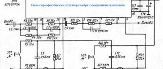
Good afternoon. I would like to clarify the values of resistors R3, R8, R14 and R18, the parameters L1 in the control electronics, the values of resistors R22 and R25 in the false panel, and whether it is possible to lay out printed circuit boards. Thank you.
Of course, respect to the author for the development! But to repeat it, you must first disenchant the power supply control circuit, which is in the PDF. Crap! What makes you encrypt the scheme first? And the one for whom it is posted here then deciphers this scheme. What kind of moron came up with this idea? Was it really impossible to properly draw both control schemes (pdf) on one sheet and without any links like: Vref, AGND... What kind of mediocrity is this. BSVi - a big disadvantage for you in drawing diagrams! You are mediocrity. Never do this again. Ask the experts to do it
Voltage regulator
As a rule, in home-made small electronic devices, power is provided by a standard PC UPS made on TL494CN. The connection diagram for the PC power supply is well known, and the units themselves are easily accessible, since millions of old PCs are disposed of every year or sold for spare parts. But as a rule, these UPSs produce voltages no higher than 12 V. This is too low for a variable frequency drive. Of course, you could try and use a higher voltage PC UPS for 25V, but it would be difficult to find, and too much power would be dissipated at 5V in the logic gates.
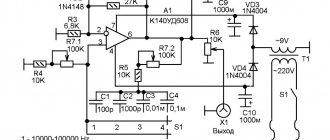
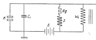
However, on the TL494 (or analogues) you can build any circuits with output at increased power and voltage. Using typical parts from a PC UPS and power MOSFETs from the motherboard, you can build a PWM voltage regulator using the TL494CN. The converter circuit is shown in the figure below.
On it you can see the circuit diagram of the microcircuit and the output stage using two transistors: a universal npn- and a powerful MOS.
Main parts: T1, Q1, L1, D1. Bipolar T1 is used to control a power MOSFET connected in a simplified way, the so-called. "passive". L1 is an inductive choke from an old HP printer (about 50 turns, 1 cm high, 0.5 cm wide with windings, open choke). D1 is a Schottky diode from another device. The TL494 is connected in an alternative way to the above, although either method can be used.
C8 is a small capacitor to prevent the influence of noise entering the input of the error amplifier, a value of 0.01uF will be more or less normal. Large values will slow down the setting of the required voltage.
C6 is an even smaller capacitor, it is used to filter high-frequency interference. Its capacity is up to several hundred picofarads.
Charging from an ATX unit on TL494 and TPS3510 – ISO-450PP
When converting a PWM TL494-based ATX unit into an ATX charger, you may encounter circuits that use a separate TPS3510 supervisor to control output voltages; WT7510 or others. Today we will show an example of how to disable such a supervisor so that it does not affect the operation of PWM in any way. And so, charging from the ATX unit CWT ATX-300 (ISO-450PP), let's go!
Charging from an ATX unit on TL494 and TPS3510
Chips like TPS3510; WT7510 monitors the voltage on several buses of the unit at once; if the voltage deviates on at least one of them, this supervisor stops the operation of the unit.
When making a homemade charger based on such a computer power supply, the main modification is to raise the voltage on the +12 bus to 14V.
If you do not disable the supervisor, the unit will operate extremely unstable, there will be malfunctions under load or problems with starting.
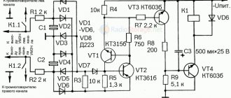
Typical block diagrams based on TL494 and TPS3510; WT7510. The diagrams already indicate some important elements; they will be discussed below.
Disabling the supervisor and organizing the unit's autostart
We will convert the CWT ATX-300 unit into a charger.
The board contains TL494 and TPS3510.
We remove diode D15, it is highlighted in the diagram with a red frame. If the block uses a different part numbering or a different circuit, we are looking for a diode that connects the 4th leg of Tl494 (DTC) and the 3rd leg of TPS3510 (FPO).
After removing the diode, the unit will start automatically when connected to the network, and the TPS3510 will no longer affect the operation of the power supply.
How to increase the voltage in the computer power supply?
The optimal voltage for charging a car battery is considered to be 14-14.5V. To increase the voltage, you need to install a trimming resistor instead of the resistor connecting the 1st leg of the TL494 to the +12V bus.
In the diagram it is highlighted with a green frame. The trimmer resistor can be taken at 100-200 kOhm (preferably multi-turn).
Before installing it on the board, it must be set to the same resistance as the resistor in its place.
After a successful start, we adjust the output voltage using a trimmer.
If desired, you can additionally make protection against polarity reversal and charging from the ATX unit is ready!