SRPP - features of work
Among amateur radio developments, the SRPP scheme is popular. However, few people understand what it is. SRPP is a single-ended cascade. Let's try to figure it out.
For analysis, let's take the SRPP circuit from the book by Morgan Jones (p. 237), exclude the capacitor-bypass cathode resistor for now and add a current sensor R5 to the upper arm.
With the same parameters of the lamps and the same resistors R3, R4, the DC arm voltage is automatically set equally. The fact that this is not a push-pull cascade, I think, is clear to a novice radio amateur.
Let's measure the shoulder currents at idle:
Since at idle there is no AC load through R4, the cascade operates as a single-cycle, the currents of both arms are equal. But the UN is not designed to operate at idle. If you look at SRPP loads in real circuits, you can find a wide range of their values from several tens to hundreds of kOhms. We reduce the load resistance until the upper arm current stabilizes. This happened with a load resistance of 33 kOhm.
Let's verify this by taking oscillograms of the arm currents:
From the oscillograms of the arm currents it is clear that the upper arm current does not change and is equal to a constant value. At the same time, the distortions introduced by the cascade have decreased slightly compared to idle operation. Let us continue to load the voltage amplifier until the arm currents are equal, i.e. to a pseudo-push-pull mode close to push-pull.
A quick analysis showed that the SRPP stage has a relatively high output impedance (in this example 6 kOhm) and is very critical to the load resistance. For example, it is known that the input impedance of a typical push-pull Darlington double when operating at a 4 Ohm load can vary from several kOhms to 80-100 kOhms. It is clear that when working with such a load, the audio frequencies will be modulated by the signal itself with a change in Kg within a wide range. In some sources you can find information that it has an increased gain due to the counter dynamic load. Actually this is not true. To verify this, let’s carry out the following comparative test of two UN:
If you look at the parameters of a simple cascade connection of OK-OA, it is easy to see that such a configuration has a lower output impedance (150 Ohms versus 6 kOhms for SRPP), a stable gain when the load resistance changes within a wide range, and a stable Kg practically independent of the load resistance . If we use a 100 kOhm resistor as a load, then in this case we have the same UA gains of 25 dB, but the SRPP-based UA introduces distortion 1.5 times (3 dB) greater.
Based on the results of the analysis, we can conclude that the SRPP cascade has much more disadvantages than advantages. The only advantage is higher efficiency, since amplification and matching with the next stage is solved by one stage, albeit unsatisfactorily. But for an audio amplifier this makes no difference. Pseudo-push-pull AC mode, close to push-pull, is obtained only at a certain load resistance. Only in this mode the cascade distortion is minimal, but at the same time the transmission coefficient drops, and the output impedance remains high, thereby leaving the danger of modulation of the amplified signal. In Morgan Jones' example, the cathode resistor of the bottom lamp is bypassed by a capacitor. Let's see what this gives.
When bypassing the lower cathode resistor with a capacitor, we have a lower output resistance (2.5 kOhm versus 6 kOhm without a capacitor) and a fairly high Kg that is slightly dependent on the load. If we compare the classic SRPP with the cascade connection of OK-OA, then the distortions introduced by SRPP are approximately 3 times higher at any load.
Analysis carried out by: Alexander Petrov , 12/12/16.
Voltage amplifier on the SRPP stage
It is often indicated in the literature that the main distortions in the UMZCH are introduced by the output transistors as the least fast ones. But this statement, in my opinion, is only true for amplifiers with deep overall negative feedback.
In them, a pulse signal of a very complex shape is supplied to the output transistors, which is the result of subtracting the undistorted input signal and the signal from the output of the amplifier with the whole “bouquet” of distortions from the amplifier and final stages. The use of separate amplification of voltage and current signals without a common feedback shows that the main distortions occur in the voltage amplifier.
The final current amplifier operating in repeater mode generates mainly switching distortion, the level of which, even in class “B” mode, usually does not exceed 0.1% and is effectively eliminated by switching to class “A” or “A+” mode. In this case, a signal close to sinusoidal, although distorted by the voltage amplifier, arrives at the final current amplifier.
Added here are the harmonics of this signal, which are also sinusoidal in shape, and even slow output transistors can easily handle them. Therefore, the main task is to obtain a voltage-amplified signal with minimal distortion.
- transistor with shallow overall feedback [1, Fig. 5];
- tube resistive stage with a cathode follower at the output [2. Fig.1];
- transformer amplifier [3];
- classic tube SRPP stage with auto-bias on a 6N23P tube (4).
All variants of voltage amplifiers were connected to a powerful current amplifier operating in class “A” mode [3]. This final stage allows you to very clearly determine the difference in the sound of all amplifiers being tested, as well as changes in the sound when adjusting the modes.
As for switching distortions, with the described voltage amplifiers, when the final current amplifier is switched to class “B” mode (only the tracking power amplifier is connected to the output) in one of the channels, it is very difficult to determine the difference in sound quality. This once again confirms that the main audible distortion occurs precisely in the voltage amplification stage.
As a result, I came up with two schemes, which I offer to the readers. One is designed for “lamp lovers” who prefer “rich”, “rich” sound, and the other is for lovers of “clean and transparent”.
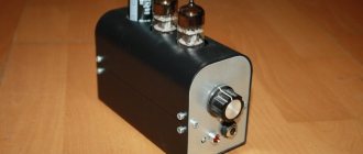
The first circuit (Fig. 1) is a modernized SRPP cascade, borrowed from [5]. The amplifying element in it can be double triodes 6N23P, 6N1P, 6N2P, 6N6P. As you know, the sound of tube circuits very much depends on the DC mode of the tubes.
To ensure the search for the “desired” sound, three practically independent adjustments have been introduced into the circuit:
- anode voltage;
- fixed bias on the amplifier triode grid;
- quiescent current.
The use of a fixed bias allowed us to eliminate the cathode resistor and large capacitor to bypass this resistor with alternating current, as is done in a classic SRPP cascade. The current source on transistor VT1 and diodes VD1, VD2 provides a stable anode current through both triodes. The magnitude of this current is regulated by resistor R5 within the range of 1.5...7 mA.
The anode voltage is supplied from a stabilizer [2], which ensures a smooth increase when turned on and is adjusted by resistor R10 within 100...220 V. For ease of adjustment, it is advisable to display all trimming resistors on the top panel of the chassis.
The use of high-quality multi-turn resistors allows you to make all settings with the amplifier turned on and immediately evaluate their impact on sound quality. It is better to heat the lamp with a rectified and stabilized voltage (6 V). The fixed bias voltage (0...5 V) is generated from -15 V, which is used for the op-amp integrators in the final current amplifier.
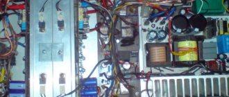
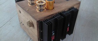
The amplifier is mounted using a hinged method using the petals of the lamp socket and additional contact pads in the form of small squares of foil fiberglass, glued to the chassis from the mounting side at the required points. The voltage stabilizer is assembled on a printed circuit board, the drawing of which is shown in Fig. 2.
The second voltage amplifier circuit is “solid-state” and is made using “Soviet” components: op-amp K157UD2 and transistors KT940A (Fig. 3). The high linearity of SRPP tube stages is generally recognized, so I decided to apply a similar solution to the transistor stage. The use of a “voltage-controlled current source” on DA1 and VT1 as an amplifying element, as well as high-voltage power supply to the transistors, are borrowed from [6].
Instead of a resistive load, a dynamic load is included on transistors VT2 and VT3. To further increase the load capacity of the amplifier, an output emitter follower\/T4 with a current source in the VT5 load was introduced. The high linearity of the amplifier is ensured by the coverage of deep feedback through DA1 of the most nonlinear element of the transistor VT1 and the creation of lightweight operating conditions using a dynamic load in the form of a composite emitter follower VT2, VT3.
To expand the range of linear operation of the amplifier transistor, the amplifier is powered by a high (160 V) “tube” voltage. Since the amplifier is not covered by a common feedback loop, the gain depends on the current transfer coefficient of transistor VT1, so it is advisable to select them identical in both channels. Fine adjustment of the gain is provided by resistor R3.
By changing its resistance (from 0 to 2.2 kOhm) you can compensate for the difference in gain up to 6 dB. When connecting the amplifier to a tube final stage, you can eliminate the output emitter follower on VT4. VT5 and increase the supply voltage of the transistors to 300 V. To drive a push-pull tube “end”, a phase-inverted amplifier from [6] is suitable.
The high-voltage power supply to the transistors is carried out from the same stabilizer as the tube SRPP. In principle, for transistors the source can be simplified, because transistors do not require a smooth increase in voltage and its regulation. Circuit R7-C3 together with R6-C2 provides a rise in low frequencies in the range of 40...80 Hz by 6 dB. If this is not required, then to eliminate the rise it is enough to increase the capacity C2 by an order of magnitude.
If necessary, you can reduce the gain of the cascade either by replacing transistor VT1 with a lower current transfer coefficient, or by introducing resistor R8, which with R7 forms an alternating voltage divider in the base of the composite emitter follower. For a two-channel voltage amplifier, a printed circuit board has been developed, shown in Fig. 4.
In the circuit in Fig. 3, the role of the zener diode VD1 in the emitter VT1 is to dampen excess negative voltage. In a signal circuit, the use of a zener diode is generally undesirable due to its increased “noisiness”. It can be eliminated by replacing it with a resistor with a resistance of 6.8...7.5 kOhm and thereby increasing the depth of the local feedback loop of transistor VT1.
The best solution is to use a current source on field-effect transistor VT6 with resistor R13 in the source circuit to select the required value of current VT1 (Fig. 5). In order not to make changes to the amplifier's printed circuit board, these elements can be placed on an additional small board (Fig. 6), which can be installed in place of the zener diode on the hard terminals perpendicular to the main board, and a jumper can be soldered in place of R10.
It is more convenient to select R13 separately. To do this, connect the board via a milliammeter to a -15 V source and by changing resistance R13 (instead, turn on a variable resistor with a resistance of 1 kOhm) to achieve a milliammeter reading of 1.4 mA. In conclusion, I would like to say that although “there are no comrades in taste and color (and I will add in sound), I prefer the sound of a transistor amplifier.