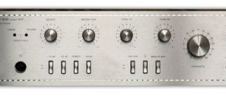
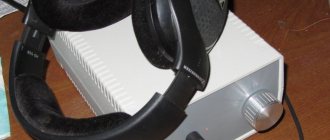
Unfortunately, the built-in telephone amplifier of the Creative E-MU 0204 USB DAC can hardly cope with my favorite TDS-5 isodynamic headphones (made in the USSR), which I have been using since the 80s of the last century.
An amplifier is needed, we need to make friends between the bourgeoisie and the Tedees. At random I found in my chests a pre-amplifier board according to the circuit diagram by Yu. Solntsev from the Radio magazine for 1985. The circuit is essentially an op-amp (K574UD1 in the original), powered by a parallel repeater on complementary transistors (KT3102, KT3107). I blew off the dust and tried this PU as a telephone one. The result was very encouraging and inspired the “reincarnation” of the scheme in an updated form.
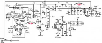
↑ Headphone amplifier circuit
Rice.
1. Original pre-amplifier circuit. “Radio”, 1985 Fragment excluded.
The full version is available to patrons and full members of the community. Description of changes in my circuit:
1. Replaced the operational amplifier K574UD1 with NE5532P, tried others.
2. I installed 2N2905 + 2N1893 as output transistors. Why? Because they fit quite well and I have a lot of them. I chose one with a gain of about 100. I had to play tricks with the radiators - I wound coils with thick copper wire, which I placed tightly on the housings. You can supply a lot of other options for output pairs, for example BD139 + BD140, they also have convenient flanges on the housings.
3. Added resistors R4, R5, by increasing which we select the desired current of the output transistors. If desired, you can drive the output stage into class A. The greater the resistance of the resistors, the greater the current and the closer the coveted class A. However, the larger the radiators will be required, and you will have to increase the current in the collectors VT1, VT2. Here an unplowed field opens up for maniacs, of which I do not consider myself. Based on the results of measurements and listening, I settled on 7.5 Ohms. In this case, the output stage current is 4 - 5 mA. And my improvised coils were quite suitable as radiators for output transistors.
4. Changed the switching circuit to inverting.
5. Reduced the AC gain due to the specific operation of telephone amplifiers from modern sources with a high (up to 2V) signal level.
6. I removed the input capacitance, since the amplifier is supposed to be used with a specific DAC, the output of which is guaranteed to have no constant voltage.
7. For power supply on the board, I installed electrolytes C2, C4 = 4700 μF x 25 V and ceramics C1, C3 = 1 μF (closer to the op-amp power terminals).
8. I abandoned the volume control, since it is at the DAC output.
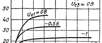
The use of a so-called “parallel” amplifier in the power amplifier [1] made it possible, with good thermal stability of the quiescent current, to do without the careful selection of a temperature-compensating circuit and adjustment of the quiescent current, traditional for push-pull output stages operating in AB mode. However, such a significant drawback of the “parallel” amplifier as the unsatisfactory amplitude characteristic did not allow the use of another of its advantages: like some other multistage amplifiers using complementary pairs of transistors, it has relatively high linearity.As it turned out, the amplitude response of a “parallel” amplifier can be improved without using a diode switch for amplification channels. In Fig. Figure 1 shows a schematic diagram of an audio frequency power amplifier (UMPA), the final stage of which (transistors VT9 - VT12) is a “parallel” amplifier. Improvements in the amplitude characteristics were achieved by using circuits R13 - R15C5 and R16 - R18C6, which act as stable current generators in the base circuits of transistors VT11, VT12. The voltages on capacitors C5 and C6 are practically independent of the signal level and are equal to approximately 8 V. The voltages on the emitter junctions of transistors VT11 and VT12 vary from 0.5 to 1.5 V, so the current, for example, through resistor R15 is almost constant and depending on the amplitude of the signal, it is only redistributed between the emitter of transistor VT9 and the base of VT11. If we exclude capacitors C5, C6, essentially implementing the output stage described in [1], then the limiting level will decrease from ±24 to ±12 V and, interestingly, the harmonic coefficient of not yet limited signals will increase by about 10 times.
The main technical characteristics of the final stage are as follows:
| Rated output power, W, into a load with a resistance of 8 Ohms | 25 |
| Nominal input voltage, V (input resistance, kOhm) | 15(4) |
| Harmonic coefficient, %, no more | 0,22 |
| Quiescent current. A | 0,25 |
| Constant output voltage in the absence of a signal, V. no more | ±0,05 |
The cascade can be used as a functionally complete unit, for example, to “amplify” existing UMZCHs or as final amplifier stages in a multi-band system with frequency division at its input.
Another possible application of a “parallel” amplifier is illustrated by a cascade on transistors VT1 - VT4. The output signals in this case are not the emitter currents of transistors VT3, VT4, but the collector currents, which are no longer directly summed up: they enter cascades similar to the so-called “current mirror” (transistors VT5 and VT6, VT7 and VT8). the only difference is that these stages additionally amplify the current by about 10 times. The connection point of the emitters of transistors VT3, VT4 is the input for the OOS signal coming from the low-resistance voltage divider R10R11C3. The feedback depth is small (about 30 dB), so the amplifier does not self-excite even without additional frequency response correction.
The signal distortion introduced by the preamplifier is very specific. If the OOS voltage stops changing, for example, due to its limitation at the output of the UMZCH, then the current of transistor VT3 or VT4 increases until it enters saturation mode. Moreover, if we exclude elements R6,VD1 and R7,VD2. the voltage at the input of the final stage from the level preceding the moment of limitation (about 21 V) will quickly decrease to approximately 1 V. As a result, instead of a limited sinusoid, a signal consisting of will appear at the output of the UMZCH. from its sections alternating with sections of constant voltage close to zero.
Thanks to the use of current limiting resistors R6. R7, the signal at the input of the final stage when transistors VT3 or VT4 is saturated is practically no different (only 0.3 V less) from the limiting level.
Main technical characteristics of UMZCH
| Rated output power, W. on a load with a resistance of 8 ohms | 25 |
| Rated power band, kHz | 0,02…200 |
| Nominal input voltage, V (input resistance, kOhm) | 1(150) |
| Harmonic coefficient, %, no more | 0,15 |
| Intermodulation distortion coefficient, % no more | 0,2 |
| Maximum slew rate of output voltage. V/μs | 15 |
| Output impedance. Ohm. no more | 0,2 |
A few words about the features of the final stage, characteristic of “parallel” amplifiers in general. When designing such amplifiers, it is necessary to take into account the areas of the emitter junctions of the transistors used. Note that the current flowing into the base of transistor VT11 (VT12) cannot exceed the quiescent current of transistor VT9 (VT10), since the current through resistor R15 (R16) is practically unchanged. It is not difficult to calculate the maximum base current of transistor VT11 (VT12), taking into account the inverse dependence of the transmission coefficient h21e on the emitter current. For an amplifier according to the circuit in Fig. 1 quiescent current of transistor VT9 (VT10) is 83 mA. Further, the quiescent current of transistor VT11 (VT12) is how many times greater than the quiescent current of transistor VT9 (VT10), how many times is the area of the emitter junction of the first greater than the similar area of the second. For example, if pairs of transistors KT814/KT815 (VT9/VT10) and KT819/KT8I8 (VT11/VT12) are used in the final stage, the quiescent current of the latter will be approximately 6 times greater.
So, in a “parallel” amplifier there are three circuits for the flow of quiescent current: R13 R15, VT9; VT10, R16—R18 and VT1I, VT12. For an amplifier according to the circuit in Fig. 1 (VT9 is equivalent to VT11, and VT10-VT12) the total quiescent current will be: 83 mA + 83 mA + 83 mA » 250 mA. Obviously, it will be the smallest if the pairs of transistors VT9/VT10 and VT11/VT12 are the same. Moreover, it is undesirable to use transistors of the KT816.KT817 series in the final stage. With the same emitter currents, their parameter h21e is significantly less than that of KT818, KT819, and this requires an increase in the quiescent currents of transistors VT9, VT10 and the amplifier as a whole. A decrease in the coefficient h21e at high emitter currents leads to the fact that in order for the amplifier to operate on a load with a resistance of 4 Ohms, the quiescent current will have to be increased not by 2 times, but by approximately 3 times. From the above, it is clear that the strong dependence of the h21e parameter on the emitter current of silicon transistors is a limiting factor for their use in a “parallel” amplifier.
The fact that the described UMZCH uses transtors of the KT818 and KT819 series has one more positive side: the amplifier can withstand a load short circuit for tens of seconds, so for its reliable protection it is enough to install fuses in the power circuits.
Despite the similarity with the known push-pull power amplifiers operating in AB mode, the “parallel” amplifier is a linear amplifier in the sense that the operating points of its transistors do not enter the collector current cutoff region (i.e., the transistors are always open). If, however, resistors with a resistance of 0.2 Ohm are included in the emitter circuit of transistors VT11, VT12. as is done in known amplifiers, their operating points will go into the collector current cutoff region, which is why the harmonic coefficient will increase significantly.
Thermal stability of the final stage is ensured by pairwise installation of transistors VT9, VT12 and VT10, VT11 on heat sinks, and the input stage due to the fairly low thermal resistance of the short terminals of the transistors and the small, moreover, approximately identical power dissipated by them.
Typically, restrictions associated with a decrease in the h21e coefficient at high emitter currents can be achieved if a composite transistor is used instead of each transistor of the final stage.
| Rice. 2 |
In Fig. Figure 2 shows a circuit of an UMZCH, in which a “parallel” amplifier is also used in a device for protecting the output stage from a short circuit in the load. The device works as follows. The output voltage of the amplifier is supplied to one of the diagonals of the measuring bridge formed by resistors R18, R19, R23 and the load Rн; a “parallel” amplifier on transistors VT15 VT18 and a symmetrical threshold element consisting of diodes VD5, VD6 connected in back-to-back parallel mode are connected to the other. Under normal conditions, the voltage between the connection points of resistors R18, R19 and R23, Rн is less than the opening voltage of the threshold element, and small (about 1 mA) direct currents flow through the collectors of transistors VT17, VT18, which do not affect the operation of the final stage. When the load is short-circuited, almost all of the voltage across resistor R23 is applied to the threshold element, one of the diodes VD5, VD6 opens and the current of the corresponding circuit (R13R14VD3 or R16R15VD4) flows through the collector of the corresponding transistor (VT17 or VT18). As a result, the current of the output stage of the UMZCH (VT13, VT14) is limited to a value less than the maximum under normal operating conditions. Capacitor C7 reduces the response speed of the protection. The fact is that it is impossible to accurately balance the measuring bridge over the entire frequency range; this is especially difficult to do in its high-frequency region. For. To improve balancing at medium frequencies, it is necessary to connect capacitor C11 in parallel with resistor R18 (shown in dashed lines in Fig. 2), the capacitance of which is selected experimentally.
The main technical characteristics of the UMZCH, assembled according to the diagram in Fig. 2 (with preamplifier), the following:
| Rated output power, W. on a load with a resistance of 4 ohms | 50 |
| Rated power band, kHz | 0,02…200 |
| Harmonic coefficient. %, no more | 0,15 |
| Intermodulation distortion coefficient, % no more | 0,2 |
| Maximum slew rate of output voltage. V/μs | 15 |
| Output resistance, Ohm. no more | 0.43 |
| Output short circuit current, A | 2,3 |
The difference between this amplifier and the previous one lies in the final stage. Transistors VT13, VT14 operate without an initial bias voltage. Resistor R17 linearizes the final stage [2]. Its functions are that with small output signals (less than 0.6 V), the AF voltage from the previous stage (VT9 - VT12) is supplied to the load, bypassing transistors VT13, VT14. As the signal increases, these transistors turn on much more smoothly with the presence of resistor R17 (R17 = 2Rн) than without it, and the harmonic coefficient of the final stage does not exceed 15% (without a resistor it is several times higher). The stage preceding the final one is subject to strict requirements: low output impedance and good linearity without an OOS circuit. Failure to comply with the first of these requirements in the amplifier [3] did not make it possible to obtain a harmonic coefficient of less than 0.5% even with an OOS depth of 60 dB.
The supply voltage of both amplifier options can be reduced to ±6 V, while their functionality is maintained.
Amplifiers can be powered with unstabilized voltages.
Construction and details. In both amplifiers, KT315V transistors can be replaced with KT315G-KT315E; K.T361V - to KT361G-KT361E; K.T3102A and KT3107A - respectively on KT3102B, KT3102E, KT3117A, K.T373A, KT373G and KT3107B, KT3107I, KT3108A. Instead of those indicated in the diagrams in the final stages, you can use transistors of the KT814, KT815, KT818, KT819 series with indexes B and V, and when the supply voltage is reduced to ±15 V - with index A. Static current transfer coefficient h21e of transistors VT11, VT12 (Fig. 1) must be at least 30.
When assembling the amplifier according to the diagram in Fig. 1, the transistors of the final stage, connected by the collector terminals to the power wire of the same name, are installed on one side of the common heat sink close to each other. Transistors VT9, VT12 and VT10, VT11 amplifier according to the circuit in Fig. 2 are mounted on plate heat sinks marked directly on the printed circuit board. They are made from sheet aluminum alloy with a thickness of 0.5...1 mm. For a workpiece measuring 40xx50 mm, a shelf 10 mm wide is bent at a right angle, in which two holes are drilled and screws for fastening to the board. For transistors of the final stages, heat sinks 8.650.022 with an effective cooling area of 300 cm2 were used.
Instead of KD522 diodes, you can use any low-power silicon diodes with a reverse voltage of at least 50 V, instead of D9A - any germanium diodes designed for a forward current of 100 mA.
A mandatory element of both amplifiers must be capacitor C2 and fuses FU1, FU2. If you plan to use an unstabilized source for power supply, connect the amplifier to the filter capacitors either with short-length conductors (less than 100 mm) or large cross-section (about 1 mm2). If this condition is not met, the harmonic coefficient increases significantly. If a stabilized source is used, capacitors with a capacity of 2000 μF must be additionally connected to the UMZCH power supplies.
Properly assembled amplifiers do not require adjustment. The only thing. what needs to be done is to balance the measuring bridge of the protection device (Fig. 2) by selecting capacitor C11 and resistor R19.
In conclusion, it should be noted that the main source of nonlinear distortions in the UMZCH according to the circuit in Fig. 2 is the voltage amplifier (VT1 VT4). The harmonic coefficient of the amplifier with an open circuit feedback loop reaches 3%. By improving the linearity of this amplifier stage, the harmonic distortion can be reduced to 0.01. 0.03%.
LITERATURE
- Ageev A. Amplifier block of an amateur radio complex. Radio, 1982, No. 8, p. 31-35.
- Zapf J., Schvenn R. Ein Okonomishes, vollgeschutztes Hi-Fi Verstarkerkonzept
- Ageev A. Thermally stable amplifier Radio, 1981, No. 7-8 p.34-35
fon 20 W bis 200 W. - Funkschau, 1977, Heft 25, z: 130 - 134
Radio 1985 No. 8
↑ How it happened
I drew a signet.
Fragment excluded. The full version is available to patrons and full members of the community.
Etched. Soldered. Inserted it into the case. I thought it was a prototype, to hell with it. So it took root.
Rice. 4 and 5. Permanent temporary building
Turned it on. I played with the modes of the output transistors. By this time, the Takstar TS-671 120-Ohm monitor headphones ordered on Aliexpress arrived. I listened. Conducted RMAA measurements. I changed the awl for soap: NE5532P to LM833N. These are inexpensive, widely used opamps of approximately the same class. I listened again and took measurements in RMAA.
I couldn’t appreciate the difference in sound due to the fact that I listened with a time gap for resoldering the op-amp (there are no panels). And you can hardly hear the difference, because the op amp is approximately the same class. What the measurements actually confirmed: the difference is within the error.
I haven’t tried other OUs because I don’t have them at hand and I can’t quickly buy them in my small town. And the concept of the amplifier “I made it from what I had” will be violated.
↑ Deep in RMAA
I know that many people do not like this program, believing that the product is designed to help marketers, so that it is easier for them to “fool” us.
But I believe that even if this is so, it is still just a tool. Good or bad, it is a tool and you need to know how to use it. Moreover, the tool is actually convenient! Measurement conditions.
The Creative E-MU 0204 audio interface has two linear mono inputs with a resistance of 1.5 kOhm and a sensitivity in the leftmost position of the controls of 6.5 dBV (2.11 Vrms rms, or 2.98 Vpp peak). I’ll put it in this position, so the manufacturer removes all the characteristics. Two stereo outputs, line and telephone, comparable in level 6.7 dBV (2.16 Vrms rms or 3.05 Vpp peak).
First I tested the telephone output of the interface (in fact, the whole mess started because of it), connecting its output directly to the linear input (loopback), and then I tested three pairs of headphones with a resistance of 120 Ohms (Takstar TS-671), 72 Ohms (TDS-5 ), 32 Ohm (Delta). A total of four dimensions. Then I connected the input of the assembled amplifier to the output of the interface and made the same four measurements from its output.
The results are summarized in the table below. I will not interpret all the results obtained - the article will be too overloaded. At the end of the article I attach *.sav measurement files, see if anyone is interested!
The results of my measurements in RMAA with interpretation
Rice. 6. Summary table of testing results
Rice. 7. RMAA level setting window
Along the way, I compared the load capacity of the interface and the amplifier by reducing the output level under load.
Rice. 8. Load capacity
Now the fun has begun. As you can see, as the load resistance decreases, the output level at the telephone output of the interface decreases. Our amplifier handles this without reducing the level.
Rice. 7a. RMAA assessment of the “interface output - line input” connection
Overall rating: “excellent”. That would be the case under load.
Rice. 7 b. RMAA assessment of the “interface output - line input” connection. Load - Takstar headphones
But no. Total harmonic distortion + noise is only “good”, and intermodulation + noise (0.264%) is only “satisfactory”. I have an assumption that this is due to incorrect operation of the program. But more on this when considering the graphs. Not good (-60.2 dB) and with mutual penetration of channels.
Rice. 7th century RMAA assessment of the “amplifier output - line input” connection. Load - Takstar headphones
The amplifier conditionally (-72 dB) failed only the mutual penetration of channels.
Rice. 9. Frequency response. The only graph where it was possible, without compromising legibility, to view the results of all eight measurements simultaneously
At six we see an even merging line. And only the interface loaded with Takstars and Deltas produces a bizarre frequency response deviation. Already, scary to say, by 0.5 dB. The impedance of the TDS is 5 linear.
Rice. 10. Intermodulation Distortion + Noise
Here we see another reason why I wanted to build an external amplifier. The remarkable curve for the unloaded output of the interface begins to bristle with harmonic peaks under load. This may be due to the incorrect operation of the level normalization program; most likely it is tied to 1 kHz. This is where we remember that rise in frequency response. Perhaps it was this that caused the clipping (the program, by the way, honestly warned with the corresponding window), which in turn led to an inexplicable increase in the level of distortion.
Attempts to disable normalization and lower the level a little did not lead to anything. Disabling normalization does not work in the free version.
The graphs of the amplifier with and without load are modestly located in the middle, allowing us to receive an excellent rating from RMAA for this parameter.
Figure 10. Interpenetration of channels
We observe the same picture of the distribution of results. The “best” and “worst” results are the interface. Amplifier - modest "good". I can imagine power problems both at the interface (power is provided via USB from the computer’s power supply) and in my amplifier, which, although powered from a stabilized rectifier, is not structurally optimal.
Figure 11. Intermodulation. Variable frequency
All the same.
Fig 12. Frequency range. Floating tone
Similar to frequency response.
Bridge-parallel amplifier
A bridge-parallel amplifier
The configuration uses a combination of bridged and parallel amplifier configurations. This is most often used with IC power amplifiers where it is desirable to have a system capable of generating more power at the rated load impedance (i.e., the load impedance used is that specified for a single amplifier), without exceeding the power dissipation per amplifier. . From the previous sections, you can see that a bridge configuration doubles the dissipation in each amplifier, while a parallel two-amplifier configuration halves the dissipation in each amplifier when operating at nominal load impedance. Thus, when both configurations are combined, assuming two amplifiers per configuration, the resulting amplifier dissipation now remains the same when operating at rated load impedance, but with nearly four times the power that each amplifier is individually capable of delivering to the load.
↑ Results
A little about the results of listening and testing. I don’t like the amplifier to introduce ad-libs in its operation, as they say, “singing,” “involving,” and so on. I don’t like all kinds of “improvers” and I think that the desire to turn the tone control arises when there are shortcomings in the sound path. Therefore, I always strive for the device to work as accurately and discreetly as possible. To my ears it worked!
I thank everyone who read to the end for their patience and forbearance. As a conclusion, I would like to say that the task of assembling an amplifier that would correspond (without fanaticism) to the level of the “Creative E-MU 0204” sound source and headphones (Takstar TS-671, TDS-5) that I have has been completed for myself and I can calm down for a while.
Recommendations
- Eiche, John F. (1990). A Guide to Sound Systems for Worship
. Recording and audio technology. Hal Leonard Corporation. paragraph 87. ISBN 0-7935-0029-X. - "Stereo, parallel and bridged mono." Amplifier Guide
. DirectProAudio. Retrieved September 28, 2011. - Roberts, Joe (2007). "Audio Power Amplifier Basics." Technical Notes by Joe
. Retrieved September 28, 2011. - Self, Douglas (2009). Audio Power Amplifier Design Guide
(5th ed.). Focal Press. item 367. ISBN 0-240-52162-5. - ^ a b
Bartlett, Bruce (1 May 2010). "Amp Power Masterclass: Not All Ratings Are Equal." ProSoundWeb. Retrieved September 28, 2011.
↑ Additions to the article. Option for beginners
Over the course of six months, I assembled several amplifier options with a parallel repeater: Report on amplifiers on the Datagor forum First - using first the recommended 2SA1930/2SC5171 in the TO-220FP package, without resistors.
Then I decided to check how this circuit would behave with the 2N2905/2N1893 in the TO-39 package, used in the version described in the article. And, having become completely impudent, I assembled a version based on the affordable BC547B + BC557B in TO-92 cases. In all cases a positive result was obtained. New printed circuit boards were not developed in versions with high and medium power transistors.
In the case of using low-power BC547B + BC557B (TO-92), I consider it a successful printed circuit board
, which made it possible to obtain a low level of interference / interference of 50 Hz and very good other parameters. Take the archive with a signet, a list of elements and an updated diagram: