Once upon a time, creating a printed circuit board (PCB) for an electronic device was just an add-on, a supporting technology to improve quality and repeatability in mass production of electronics. But this was at the dawn of the development of electronics. Now the creation of software is a whole separate branch of technical art.
As Wikipedia says, PP is:
A dielectric plate on the surface and/or in the volume of which electrically conductive circuits of an electronic circuit are formed. A printed circuit board is designed to electrically and mechanically connect various electronic components. Electronic components on a printed circuit board are connected by their terminals to elements of a conductive pattern, usually by soldering.
Today, radio amateurs have access to factory production to order their printed circuit boards. It is enough to prepare the necessary files with a printed circuit board design and additional information about holes, etc., send it to production, pay and receive ready-made factory-quality PCBs with silk-screen printing, solder mask, precisely drilled holes, etc. Or you can make PP the old fashioned way at home using LUT and a cheap etching solution.
But before you make a PP, you need to draw it somehow. Currently, there are dozens of programs for these purposes. They can be used to design both single-layer and multi-layer printed circuit boards. In RuNet, the Sprint Layout program is most widespread among radio amateurs. You can draw PP in it as in a graphics editor. Only your own specialized set of drawing tools. This program is simple, convenient and a good place to start your acquaintance with PCB design in CAD.
It's not my goal to create a complete guide. There are a huge number of SL tutorials on the Internet, so I will try to give a concise description so that you can quickly get down to business - drawing a printed circuit board, so I will try to talk about some useful SL functions that are really needed when creating a PCB.
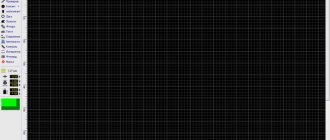
General view and working area
I recommend finding the distribution kit of this program and familiarizing yourself with the windows and properties of the program. This will help you master it faster.
The program itself looks like a regular Windows application: at the top there is a strip with the program menu (file, actions, board, functions, service, options, help). On the left is a panel with tools that are used when drawing a printed circuit board. On the right is a window that displays the properties of the working field, a specific track, a specific group of tracks, etc. Those. If you select an object on the PP, its properties will be displayed in the window on the right. A little further to the right of the “Properties” window is the “Macros” window. Macros are a convenient tool for grouping and reusing previously drawn parts or parts of a board. I will dwell on them in more detail, since they save incredible time and reduce the number of errors on the board.
Working field
The black mesh field is the working field. This is where you will place contact pads, holes for radio components and draw tracks between them. The field also has some properties. The obvious ones are length and width. The field size determines the maximum size of the PP. In this case, the width and length are specified in millimeters. This is an important clarification, since the grid cell size is set by default not in millimeters, but in mil (i.e., not metric, but inch units):
This strange measure of length came to us from England and is equal to 1/1000 of an inch: 1 mil = 1⁄1000 inch = 0.0254 = 25.4 microns
Mil is widely used in electronics, but in Sprint Layout you can configure the grid to be displayed in mm. Install it the way that is most convenient for you. Mil is a smaller measure and therefore allows you to more accurately position the elements of the printed circuit board on the working field.
Drawing functions
In the first part of the Sprint Layout course, we got acquainted with the program interface. We'll start the second part of the course by looking at what functions the program for drawing circuit boards provides.
All elements are located on the left panel.
Let's look at them.
Cursor
Hotkey "Esc".
The default tool. Used to select elements on the workspace. Resetting any tool to the “Cursor” is done by clicking the right mouse button.
Scale
Hotkey "Z".
The cursor changes to a magnifying glass. Clicking on the left mouse button on the working field increases the scale of the board, and clicking on the right mouse button decreases it.
Also, with the left mouse button held down, you can select the area of the board that needs to be enlarged.
Track
Hotkey "L".
A tool for drawing a path of a given width. The width value (in mm) is set before starting drawing in the special field below:
The button on the left opens a submenu of frequently used, so-called “favorite” track widths. You can add a new value or remove an existing one:
Note - The item to add a new value becomes active only if the current track width value is not in the list.
After setting the width, selecting the “Path” tool, you can start drawing the path directly. To do this, in the work field, select the point where the line will begin, click the left mouse button and draw the line to the point where it should end.
The type of track bend is changed by pressing the Spacebar. Five options are available:
When you press the “Space” key while holding down the “Shift” key, the search is performed in the reverse order.
During the drawing process, you can, if necessary, fix the line by clicking on the left mouse button, thereby forming the required shape of the track.
The length value is displayed for the last unfixed segments.
By holding down the “Shift” key you can temporarily make the grid step half as large, and by holding down “Ctrl” you can disable snapping the cursor to the grid.
Having fixed the last point of the track, you can finish drawing the track by clicking on the right mouse button. The track ends and the cursor is ready to draw the next track.
When you select a drawn line, it is highlighted in pink and the properties panel changes appearance, displaying the path parameters:
In this panel you can change the value of the line width, view its length, the number of nodes and the calculated maximum allowable current.
Note - Calculation parameters (copper layer thickness and temperature) are configured in the “Imax” section of the main program settings (see the first part of the cycle).
The blue circles represent the nodes of the track. And in the middle of each track segment you can see blue circles - the so-called virtual nodes. By dragging them with the mouse cursor you can turn them into a full-fledged node. Note that during editing, one segment is highlighted in green and the other in red. Green color means that the segment is horizontal, vertical or at an angle of 45°.
The ends of the tracks are round by default, but there are two buttons in the properties panel that make them rectangular (note the left end of the track).
If one trace is represented on the board by two separate tracks and their end nodes are located at the same point, then the tracks can be connected.
To do this, right-click on the end node and select “Connect Line” from the context menu. The track will become solid.
The “Negative” checkbox forms a cutout from the track on the Auto-ground polygon:
Contact
Hotkey "P".
A tool for creating pads for component pins. By clicking on the small triangle on the left, a contact menu opens where you can select the desired contact form:
The item “With metallization” makes the contact pad on all layers of copper, and the hole is metallized. In this case, the color of the contact with a metallized hole differs from those without metallization (note the round blue contact). The F12 hotkey enables/disables metallization for any selected contact.
The shapes of the contact pads are not limited to this list - they can be made in any shape. To do this, you need to place a regular contact (1), and draw a pad of the desired shape around it (2). Moreover, you should not forget about the mask - you must manually open the entire contact (3) from it (see below about the mask).
Like the “Track” tool, this tool has its own settings at the bottom:
The upper field specifies the diameter of the contact pad, the lower field specifies the diameter of the hole. The button on the left opens a submenu of frequently used contact sizes. You can add a new value or remove an existing one:
Having set the necessary values, select the “Contact” tool and left-click the mouse to place the contact at the desired point in the working field.
The settings of any selected contact (or group of contacts) can always be changed in the properties panel:
The last item with a checkmark turns on the thermal barrier at the contact. We'll look at this feature in more detail in the next part of the course.
If the contact pad does not have a warranty belt, i.e. The diameter of the hole is equal to the diameter of the contact pad, then it is displayed as follows:
SMD contact
Hotkey "S".
A tool for creating rectangular contacts for surface mount components. Settings:
On the right are fields for entering the width and height of the contact. Below them is a button for changing the values in these two fields. The button on the left opens a submenu of frequently used contact sizes.
Having specified the required dimensions and selected this tool, the contact can be placed on the working field:
For an SMD contact, the thermal barrier function is also available in the properties panel, with the only difference that it can be configured only on one layer.
Circle/Arc
Hotkey "R".
Primitives - circle, circle, arc.
We select the placement point and, holding the left mouse button, move the cursor to the side, thereby setting the diameter of the circle.
Note that the properties panel as you draw contains information about the circle being created. By releasing the left mouse button, we complete the creation of the circle. By selecting it with the “Cursor” tool, we can edit the properties of the circle in the properties panel - in particular, set the coordinates of the center, line width and diameter, as well as the angles of the start and end points if we want to turn the circle into an arc.
You can also turn a circle into an arc by dragging the cursor over the only node on the circle:
The “Fill” checkbox makes a circle out of a circle, filling the inner area, and “Negative”, by analogy with a path, turns the element into a cutout on the Auto-ground polygon.
Polygon
Hotkey "F".
A tool for creating areas of any shape. Drawing occurs along a path with a given width:
Once completed, the polygon is displayed with a fill and, when selected, the nodes can be edited (same as in the path tool):
The properties panel contains some more settings:
You can change the width of the contour line, see the number of nodes, make a cutout from the polygon using the Auto-earth fill (check “Negative”), and also change the type of polygon fill from solid to mesh.
The thickness of the grid lines can be left as the polygon outline, or you can set your own value.
Text
Hotkey "T".
Text label creation tool. When you select it, the settings window opens:
- Text – input field for the required text;
- Height —height of the text line;
- Thickness - three different types of text thickness;
- Style - text style;
- Rotate by —rotate the text by a certain angle;
- Mirror - flip text vertically or horizontally;
- Automatically - additionally add a number after the text, starting from a certain value.
Three types of text thickness and three types of style give nine style options (though some are the same):
Note - By default, the minimum possible text thickness is limited to 0.15 mm. If the thickness is too small, the text height is automatically increased. This limitation can be disabled in the program settings menu (see the first part of the series).
Rectangle
Hotkey "Q".
Tool for creating a rectangular outline or rectangular polygon. To draw, click the left mouse button in the work field and, without releasing, move the cursor to the side, setting the shape of a rectangle.
The creation of the rectangle will be completed after the button is released.
As I already said, two types of rectangles are available - in the form of an outline from paths and with a fill.
Moreover, a rectangle in the form of an outline is nothing more than an ordinary path laid in the shape of a rectangle, and a rectangle with a fill is a polygon. Those. Once created, they can be edited as a track and a polygon, respectively.
Figure
Hotkey "N".
Tool for creating special shapes.
The first type of figure is a regular polygon :
Bisector settings are available - the distance from the center to the vertices, the width of the track, the number of vertices, and the rotation angle.
The “Vertex” checkbox connects opposite vertices to each other (middle picture), “Fill” – paints the interior space of the figure (right picture):
It should be noted that the result is elements consisting of tracks and a polygon. Therefore, they are edited accordingly.
The second type of figure is a spiral :
By setting the parameters, you can create a round or square spiral:
A round spiral consists of quarter circles of various diameters, and a rectangular spiral is a track.
The third type of figure is form :
The settings allow you to set the number of rows and columns, the type of numbering, its location, and the overall dimensions of the form. Result:
The form also consists of simpler primitives - track and text.
Mask
Hotkey "O".
Tool for working with solder mask. When using it, the board changes color:
The white color of the elements means that the area will be open from the mask. By default, only the contact pads are exposed to the mask. But left-clicking on any element of the current copper layer opens it from the mask (in the picture I opened a path from the mask in the center of the picture). Pressing it back again closes it.
Connections
Hotkey "C".
The tool allows you to establish a virtual connection that is not broken when moving or rotating components between any contacts on the board.
To delete a link, you need to left-click on it with the Link tool active.
Highway
Hotkey "A".
A primitive autorouter. Allows you to trace placed “Connections”.
To do this, set the routing parameters (track width and gap) and hover the cursor over the connection (it will be highlighted) and click the left mouse button. If it is possible to lay a route with the specified parameters, then it will be laid:
In this case, the automatically laid route will be displayed with a gray line in the center of the track. This makes it possible to distinguish them from manually laid routes.
Clicking the left mouse button again with the Route tool active on the automatically routed route deletes it and returns the contact link.
Control
Hotkey "X".
The tool allows you to see the entire routed circuit by highlighting it:
Note - in the first part of the course I described setting the type of this backlight: flashing/non-blinking Test mode.
Meter
Hotkey "M".
By holding down the left mouse button, a rectangular area is selected, and a special window displays the current coordinates of the cursor, changes in coordinates along two axes and the distance between the start and end points of the selection, and the diagonal angle of the selection rectangle.
Photoview
Hotkey "V".
A handy tool that allows you to see what the board will look like after manufacturing:
The Top/Bottom switch changes which side of the board is displayed.
Note - The bottom layer is mirrored when displayed compared to how it appears when traced. The PhotoView tool works in the same way as if you were twirling a finished board in your hands.
The “With components” checkbox enables the display of the marking layer, and the “Translucent” checkbox makes the board translucent - the bottom layer is visible through it:
Two drop-down menus - “Board” and “Solder mask” change the color of the mask and the color of the contacts not covered by the mask:
Note - The “—” item displays the contacts as covered with a mask.
Macros
A macro is a saved section of the board, ready for further reuse. In Sprint Layout, a library of component footprints is organized in the form of macros.
After starting the program, by default the macro panel is open on the right. Opening/closing this panel is controlled by a button on the toolbar on the right side of the window:
This library is currently empty.
To connect the downloaded set of macros, just unpack it and place it in the folder specified in the SL6 settings (see the first part of the series):
After this, the program, having scanned this folder during the next launch, will display macros in the panel:
To delete a macro from the library, just select it in the library tree and click on the trash can icon next to the save button.
To edit a macro, you need to drag it onto the work field, make the necessary changes and, having selected the necessary elements, click on the “Save” button and save it as a new macro, giving it a name (or replace the existing one).
IPC-7251 and IPC-7351
I would like to say a few words about naming your macros. There are foreign standards IPC-7251 and IPC-7351, which determine the sizes of contact pads and types of footprints for various standard cases. But in our case, we will need recommendations on naming the footprints from there.
Let's look at the example of a 100 nF capacitor of the B32922 series from EPCOS:
According to the IPC-7251 standard, the name of its footprint will be formed as follows:
CAPRR + Lead spacing + W Lead thickness + L Case length + T Case thickness + H Case height
Therefore, according to the datasheet we have:
CAPRR_1500_W80_L1800_T500_H1050
CAPRR – Capacitor (CAP), non-polar, radial (R), rectangular (R) 1500 – Lead spacing = 15.00mm W80 – Lead thickness = 0.80mm L1800 – Case length = 18.00mm T500 – Case thickness = 5.00mm
The following parameter is optional and has no meaning for Sprint Layout:
H1050 – Case height = 10.50mm
Thus, this type of naming, after getting used to it, will allow you to find out information about the footprint by the name of the macro and avoid confusion in the library.
I have attached excerpts from the standards to the article:
- Footprint Naming Convention. Surface Mount - for SMD components.
- Footprint Naming Convention. Through-hole - for output components.
Creating Macros
As an illustrative example, we will select a circuit for which we will create a library of macros. Let this be a simple tone control on the TDA1524A chip:
Let's carefully look at the diagram and make a list of components for which we will need macros:
- Chip TDA1524A.
- Fixed resistor with a power of 0.25 W.
- Variable resistor.
- Electrolytic capacitors.
- Film capacitors.
- Connectors for connecting power, as well as for connecting a signal source and load.
- Miniature switch.
The process of creating a macro consists of several steps:
- Arrangement of contacts.
- Drawing graphics for the marking layer.
- Saving the macro in a separate file on disk.
In the video below I will show you the process of creating macros for elements of the selected diagram in two ways.
Attached files:
- Footprint Naming Convention_ Surface Mount Components.pdf (39 Kb)
- Footprint Naming Convention_ Through-hole Components.pdf (103 Kb)
Sprint Layout Toolbar
Cursor (Esc) is a common tool that is used to select an element on the PP: a hole or part of a track.
Scale (Z) - used to increase/decrease the size of the printed circuit board pattern. It is convenient when there are many thin paths and you need to highlight one among them.
Track (L) - Used to draw a conductive track. This tool has several operating modes. More on them later.
Pin (P) - The tool is designed to draw vias. You can select the shape of the hole, and also set the radius of the hole itself and the radius of the foil around it.
SMD contact (S) - for designing PCBs using SMD components. Draws contact pads of the required sizes.
Circle / Arc (R) - to draw the conductor in the shape of a circle or arc. It can be convenient in some cases.
Square (Q) , Polygon (F) , Special Shapes (N) - tools for creating areas and areas of a certain type.
Text (T) - to write text. You can set how the text will be displayed on the board: normally or mirrored. This helps to display correctly on the board, for example when using LUT.
Mask (O) - for working with a solder mask. By default, when you turn on this tool, the entire board, except for the pads, is “covered” with a solder mask. You can arbitrarily open/close any contact or track with a solder mask by clicking on it with the left mouse button.
Jumpers (C) are a virtual connection that is preserved during any manipulation of the contact tracks between which it is installed. When printing, the jumpers are not displayed in any way, but they are used for auto-routing.
Autorouter (A) is the simplest autorouter. Allows you to lay contact paths between contacts using arranged connections. In order to distinguish automatically laid paths from manually laid ones, SL draws a gray line in the middle along such a path.
Test (X) is the simplest control tool. It can be used to highlight one specific track in a layer. Convenient for checking the correct layout of tracks.
The Meter (M) is a handy tool for measuring distances on a board drawing. The meter shows: cursor coordinates, changes in cursor coordinates in X and Y, the distance between the start and end points and the diagonal inclination angle of the rectangle constructed from the start and end points of the meter.
Photo view (V) - shows approximately what your board should look like after industrial manufacturing.
Sprint Layout 6 - PCB design for electronic devices
Sprint Layout 6 is a simple and efficient software for hand-designing and drawing printed circuit boards for low to high complexity electronic devices.
Many radio amateurs often have a question: how can you quickly and efficiently draw a printed circuit board? - here the Sprint Layout 6 program will come to our aid, which is a simple and intuitive graphic editor designed for laying out and drawing printed circuit boards.
Rice. 1. Appearance of the window of the running Sprint Layout 6 program.
Perhaps the main criterion for the popularity of this program is its intuitive interface, which you can start working with without even reading the program documentation.
Sprint Layout contains quite a lot of additional tools and capabilities, for example, there is a built-in router that will help you lay out tracks (not fully automatically) and then check their correctness.
Another big advantage of SprintLayout is its extensive library of various electronic components. If you don’t find the radio-electronic component you need in the program, you can draw them yourself and then save them in the library for later use.
Sprint Layout 6 perfectly supports the *.lay file format from the previous version of Sprint Layout 5. Please note that files created in version 6 cannot be opened in the program of version 5!
The program is perfect for layout and manufacturing of printed circuit boards using LUT (Laser-Ironing-Technology) technology. Inside the program, a printed circuit board design can be rotated, mirrored, scaled, and sent to a printer for printing.
If you need to design a fairly complex electronic device with a large number and density of electronic components, then the Sprint Layout program is clearly not the best option; here it is better to look towards DipTrace and similar CAD programs with broader and more professional functionality.
In the 6th version of the Sprint Layout program, which is presented here, some additions were made by domestic enthusiasts, and the entire interface was translated from English and German into Russian, and a large number of electronic components were added. Attention!!! Essentially this is Sprint Layout version 5 but with some changes.
The program has been tested and works reliably under OS: Win98, WinNT, Win2000, WinXP, Win7, Win8. It is also possible to run the program under the Linux operating system using the Wine software package or in VirtualBox (Qemu) where any of the above-listed operating systems of the Microsoft Windows family is installed.
SprintLayout is a paid software product (Shareware).
Official website of the program: www.abacom-online.de/uk/html/sprint-layout.html
Additional components on the official website: www.abacom-online.de/uk/html/bibliotheken.html
The translation and repack were carried out by users of the RadioKot website. RePack & Russification: Men1 & Sub. Alternative RePack & Russification: UA3WM. There are more than 15,000 macros in the macros folder, so you'll probably find everything you need. Please read the ReadMe.txt file before starting. If you are not satisfied that the program takes a long time to launch, you can delete macros that you do not need in the Makros folder, the launch will be faster.
Layers in Sprint Layout
SL allows you to draw multilayer PCBs. For home purposes, you are unlikely to go beyond a 2-layer board. But if you order from production, then Sprint Layout has the necessary capabilities for rendering a board with several layers. There are seven in total: two outer copper layers (top and bottom), two silkscreen layers for the outer layers, two inner layers, and one non-printed layer for drawing the outline of the board.
Working with layers is similar to working with layers in Photoshop or GIMP (If you haven’t used gimp, I recommend it. It’s like Photoshop, only free): you can place tracks in different layers, turn layers on and off, etc. Switching the working layer and controlling visibility is done at the bottom of the working field using this control:
Each layer in SL has its own purpose:
- M1 - top layer
- K1 - marking of elements of the top layer
- B1 - inner layer
- B2 - another inner layer
- M2 - bottom layer
- K2 - marking of elements of the lower layer
- O - layer for drawing the contours of the board
When creating your board, you should remember that the text and elements in the M2 layer must be reflected. Usually SL automatically makes the text reflected, but you should still check from time to time.
When working in SL, only one layer is always active. It is on this layer that all contact pads and tracks will be placed. While working with this layer, all other layers are considered inactive - tracks and contacts on them cannot be changed.
RUSSIAN WARSHIP, FUCK YOU!
Beginning radio amateurs always face the question: “how to make a board?” In terms of technology, there are many different methods, from LUT to the use of photoresist. But first you need to somehow create the board design itself. I'm using Sprint Layout 5.0. There are many similar programs on the Internet, both better and worse in functionality, so the choice is yours.
So, let's begin. Sprint-Layout 5.0 is a simple program for creating double-sided and multilayer printed circuit boards. The program includes many of the elements necessary in the development of a complete project.
Part 1. What we have
Download the Sprint Layout program itself
This is the working field itself, so let's customize it as we like. Click “Options” -> “Settings”
And what we see:
Visualization
In general, everything is clear here.
We can set the measurement system and some settings in terms of design and management in the program itself. Colors
Here we set the colors for the working field and individual layers. We do it in a way that is pleasing to the eye. In general, I can only recommend leaving the desktop background itself black so that your eyes don’t get tired. Choose according to your taste You can save the settings themselves and then simply select them from the drop-down menu.
Directories Library
Everything is simple here.
In these bookmarks we set the path to export files in formats that are suitable for industrial production of boards and library files that we will use in the process of creating the workpiece itself. We can set it up, but I see no reason to do so. Let them be Return
Here you set the number of actions that will be saved.
Essentially this is the number of actions that we can undo (max. 50). A useful thing for low-power computers. Imax
The bookmark is needed for the calculator.
In the process of selecting the thickness of the conductor in the “Properties” panel (on the right), we will see a calculation of the maximum current that can flow in such a conductor. Useful thing Keyboards
If you are used to using hotkeys in programs, then this bookmark is for you. Here you can set the action for the button.
Well, we’ve set everything up for ourselves, let’s take a look at the program itself.
Part 2. What and where we hide and why we need it
Let's start from the top panel
- File New, Open, Save, Save As, Printer Settings..., Print..., Exit
Everything is clear with this brethren.
Save as macro
This option allows us to save a selected fragment of a diagram or other parts as a macro, which has the .lmk extension, so as not to repeat the steps to create them again in the future.
The saved part will appear in the library. Autosave
In this option, you can configure the autosave of our files with the .bak extension and set the required interval in minutes.
Export
In this option, we can export to one of the formats, i.e. save our scarf as a picture, as a gerbera file for further transfer to production, save as an Excellon drilling file, and also save as contour files for subsequent creation of a scarf using a CNC machine.
Usually useful in preparation for factory production. Directories
In this option we can configure parameters for working with the program, such as keyboard shortcuts for file locations, macros, layer colors, etc., etc. (already been above)
— Editor
Undo, Restore, Copy, Cut, Paste, Delete, Select all Everything
is also familiar and standard.
Duplicate
Quickly duplicate the selected part.
Although, ctrl+C ctrl+V is more common. Copies...
When you select this item, the following window will open: In which we can specify how many copies of the selected part we need to make horizontally and vertically and how to arrange them, either in tiles or just in a row. Convenient when you need to stamp the matrix of something.
- Project
Add a board...
Here we can add another board to our file.
Convenient when we are doing a project with several elements. Board properties...
In this option we can configure the properties of our board, such as height and width, and also give it a name, for example “Like a puff”.
Although it’s easier to do this in the “Properties” tab: Copy board
In this option we can copy our board in order to make small changes on the copy, for example, put a slightly different connector somewhere.
Remove the board
- and so everything is clear
Install last, Install first, Move the board to the right, Move the board to the left
This is to shuffle the order of boards in the drawing.
Almost useless feature. Import from...
In my opinion, the most useful option because it allows you to insert another scarf from those created earlier into the scarf, for example, it helps a lot when you drew a complex body but forgot how to save the macro.
- Action
Rotate, Mirror horizontally, Mirror vertically.
I think no explanation is required.
Unless the rotation is done at a fixed angle, which is set in the options, and the details are mirrored on the same layer. Like the picture. Group, Ungroup
You can link parts into blocks.
Thus, for example, you can create a macro. And when copying, objects are grouped. Sometimes it infuriates, and sometimes I like it. It depends on the situation. Move to opposite layer
- moves the part to the corresponding layer on the other side.
Copper on copper, silk on silk. Move to layer
- Similar to the top menu, but with a slight difference, it allows you to directly select the layer where we will move our part.
Snap to grid
In my opinion, this is a very convenient feature.
In the program, when you draw a scarf with different details, each has its own pin spacing and when you lay conductors between them. Moreover, you can set any grid in two clicks. Delete virtual connections
The Sprint-Layout program has such a feature as air connections.
Usually they denote jumpers, for example, between two holes, first put two patches, make a connection between them, it will be a thin green line, and then on another layer draw a path between these two patches, and select this option, then the program will analyze the normally connected patches and will remove all unnecessary air connections. Delete elements outside the working field
The entire working screen with a grid in the program is considered as a board, so if some element falls on its border, then this item simply deletes everything that goes beyond these boundaries.
Restoring the mask...
The mask is used on factory boards. This is the same “green paint” that is used to cover the boards at the factory, leaving only the solder contacts exposed. If you take off the mask and give it to the factory, then you will get hellish hemorrhoids with this varnish scratching all over the contact pads. Ripping it off is not an easy task and is very tedious.
— Options
Settings...
Basically, the first place we went to was
Properties.
If we select this item, then a Properties window will open on the right side of the program where we can set the size of our scarf in width and height, as well as its name.
DRC control
When we select this item, another window will open on the right which will allow us to control our drawn scarf, set restriction gaps, etc.
The point is. For example, we set a minimum gap of 0.5mm and a minimum track of no less than 0.5mm, and during the DRC check the program will find all the places where these standards are not met. And if they are not fulfilled, then there may be mistakes in the manufacture of the board. For example, the tracks will stick together or some other problem. There is also a check of hole diameters and other geometric parameters. Library
When you select this item, we will see another window on the right side of the program.
Namely, a window with macros, that is, a window where we can select our finished parts and cases for their subsequent insertion into our scarf. Template...
If you select this item, you will see the following window: A very interesting item, it allows you to put a picture as a background on our table in the program where we draw a scarf.
We will dwell on this point later. On the workfield there are buttons for quickly calling up these windows: Metallization
When selecting this option, the program fills the entire free area with copper, but at the same time leaves gaps around the drawn conductors.
These gaps can sometimes be very useful to us, and with this approach the board turns out more beautiful and more aesthetically pleasing. To change the gap, you just need to select the desired element and change the indent in the metallization properties, as in the picture: Entire board
Select this option, zoom out on the screen, and we will see our entire board.
All components
Similar to the top point, but with the only difference that it will reduce the scale depending on how many components are scattered across our scarf.
All selected
This item will adjust the screen size up or down depending on what components are currently selected.
Previous scale
Return to the previous scale, everything is simple here.
Refresh Image
A simple option simply refreshes the image on our screen.
Useful if there are any visual artifacts on the screen. Sometimes there is a glitch like this. Especially when copy-pasting large pieces of the circuit. About the project...
If you select this option, you can write something about the project itself, and then remember, especially after yesterday,
Hole table...
Quite an interesting menu item that displays how many holes are on our board and what drills are needed to drill them.
Macro creator...
Here we can select and configure the drawing of our case, looking at the data from the datasheet for a particular chip.
We select the type of sites and the distance between them. Type of location and oops! The board has a ready-made set of pads. All that remains is to design them on a silk-screen printing layer (for example, frame them) and save them as a macro. All! the following items such as Registration
and
Help
. In principle, there is nothing interesting there that could be useful to us.
Now let's turn our attention to the panel that is located on the left
Well, in general, everything is immediately clear here. A set of the most common elements needed on boards, so poke around in the program, everything is intuitive there.
Part 3. Small examples
Let's create a macro
For an example, let's take a datasheet within the reach of I have an Atmega32 and open a page with dimensions:
We see a lot of books, half of which we don’t need. And so, we open the macro creator, and we see this window:
What do we see? And we see the contacts in one row, but we need a four-sided housing, so in the drop-down menu we click “Four-sided QUAD” and fill out all the fields as in the picture:
Click on the OK button. Our body turns purple and is tied to the mouse, and then we click anywhere on the screen. All that remains for us is to make a mess by adding silk-screen printing. Don’t think that we will have to do this all the time.
Let's add this to the library. 1. Select our chip. 2. Click “File” -> “Save as macro” Z.Y. Since our case is TQFP, and there is no such thing in standard libraries, create a folder with that name and save it there. Our folder will appear in the library in the form of a bookmark: That's all, our case for the TQFP-44 microcircuit has been created, now, if anything, you can print it out, attach the microcircuit to a piece of paper, and if it’s a little wrong, then slightly correct it. Rendering a picture
I will tell you how to make a board from an image of a board found in a magazine or on the Internet. In order not to search for a long time to repeat, let’s go online and type “Printed circuit board” in a search engine and select something just like that. Here's what I took, just as an example: Z.Y. I didn’t make this device, I didn’t even understand what it was. Z.Y.Y. The image must be in BMP format.
We have dimensions in the picture of 25x100mm. Let’s draw a contour using these dimensions on the “F” layer using the “Measurement” tool. In the “Template” tab, click the Load button... and select our file. After this, our screen will look like this: That’s all, now we’ll just outline this picture with details. There are quite possible cases when the details may not fit 100% into what is drawn in the picture, this is not scary, the main thing is that there is a picture on the background layer and a set of macros with a fixed size, and this is the most important thing. Here's what I got:
Part 4. How to print?
I think that it will not be difficult for a person who has sat at a computer at least once to find such a button “”.
A window with printing settings appears: 1
Select the layer that we will print.
The main thing is not to forget to make it black. 2
Using this tab we can print only the mask or the holes themselves.
It will be useful for people who can make a mask for a fee. 3
Printing options.
The most useful thing, it seems to me, is the “Negative” checkbox, which is useful if the boards are made using negative photoresist. 4
Here you can call up standard printer properties (same as in other programs), print more than one board on one sheet, etc. I think the most useful button is “Correction” if the printer deforms the image when printing.
If I find other goodies, I’ll write here right away.
Good luck with creating your own boards for your projects.
»
- Zalognik's blog
Macros and element libraries
Each electronic component has its own dimensions, its own number of pins, etc. You won’t draw them by eye every time, especially since there are macros and entire libraries of macros for this with already verified and prepared components.
Macros are a small piece of PCB board that you can use multiple times. In Sprint Layout, you can turn anything into a macro and then reuse it over and over again in other projects. Very useful and convenient.
Macros can be combined into libraries. At the same time, the library is just an ordinary folder in which a bunch of macros are piled up, which are interconnected by some kind of logic. For example, these are smd resistors or Soviet operational amplifiers, etc. Macros and libraries are most often located in the root folder of the SprintLayout/MAKROS/ program
The process of creating a macro is very simple:
- We arrange contacts
- In the marking layer we draw a graphic designation of the component
- Save the macro
Radio communication
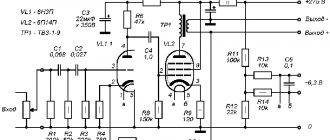
We see that the old scheme has gone through a lot of things, including corrections with a pencil and filling with alcohol rosin flux, but for our purposes it is ideal because of its simplicity. Before we draw our scarf, we will analyze the diagram to see what parts we will need.
- Two microcircuits in DIP packages with 14 legs for each microcircuit.
- Six resistors.
- One polar capacitor and two regular capacitors.
- One diode.
- One transistor.
- Three LEDs.
Let's start drawing our details, and first we'll decide what our microcircuits look like and what dimensions they have.
This is what these microcircuits look like in DIP packages, and their dimensions between the legs are 2.54 mm and between the rows of legs these dimensions are 7.62 mm. Now let’s draw these microcircuits and save them as a macro, so that we don’t have to draw again in the future and we will have a ready-made macro for subsequent projects. We launch our program and set the active layer K2, the size of the contact pad is equal to 1.3 mm, its shape is selected “Rounded vertically”, the width of the conductor is equal to 0.5 mm, and the grid pitch is set to 2.54 mm. Now, according to the dimensions that I gave above, let’s draw our microcircuit.
Now let's check its dimensions. However, if you do it on a grid, this is not required. Where does it go from the submarine?
Everything worked out as planned. Then we will save our future payment. Click on the floppy disk icon and enter the file name in the field. We have drawn the location of the legs of the microcircuit, but our microcircuit has some kind of unfinished look and looks lonely, we need to give it a neater look. We need to make a silkscreen outline. To do this, switch the grid pitch to 0.3175, set the conductor thickness to 0.1 mm and make layer B1 active.
Now click on the Explorer icon and draw a small outline, click the left mouse button when you need to put a point, and right-click when you need to complete the line, then click on the Polygon icon and make a small triangle on the left side of this outline.
With this triangle we will indicate where we will have the first pin of the microcircuit. Why did I draw it this way? Everything is very simple, in our program by default there are five layers: layers K1, B1, K2, B2, U. Layer K2 is the soldering side (bottom) of the components, layer B1 is the marking of the components, that is, where to put something or a silk-screen printing layer that can then be applied to the front side of the board. Layer K1 is the top side of the board if we make the board double-sided, respectively, layer B2 is the marking or silk-screen printing layer for the top side and, accordingly, layer U is the outline of the board. Now our microcircuit looks neater and neater. Why do I do this? Yes, simply because I’m depressed by boards that are made haphazardly, and sometimes you quickly download a thread from the network, and there are only contact pads and nothing else. I have to check every connection according to the diagram, what came from where, what should go where... But I digress. We made our microcircuit in a DIP-14 package, now we need to save it as a macro so that later we don’t have to draw something like this, but simply take it from the library and transfer it to the board. By the way, you are unlikely to find an SL5 without macros at all. Some minimum set of standard cases is already in the macros folder. And entire sets of macro-assemblies circulate on the network. Now hold down the left mouse button and select everything we just drew.
Then click on the lock icon to group them. It’s better to remember the hotkeys and use them.
And all our three objects will be grouped into one. After that, select File, Save as macro...
And let's give it the name DIP-14. It also doesn't hurt to create a tree of folders in the macros directory. And don’t dump all the assemblies into one trash heap, but sort them into sections. Now click on the macros button:
Here is the letter M on the microcircuit. And let's look at our just created macro in the macro window
Our newly created macro is displayed in the window at the bottom right. Now you can simply drag it from there onto the grid with the mouse.
Great, but it wouldn’t hurt to decide what size our board would be. I figured out the dimensions of the parts and how they could be roughly scattered and calculated that in the end my size was 51mm by 26mm. Switch to layer U - the milling layer or board border. At the factory, they will go through this contour with a milling cutter during manufacturing.
Set the conductor thickness to 0.1 mm
Choose a grid pitch equal to 1 mm
And we draw the outline of our future board.
An observant person will say, yeah, the starting point of the contour does not lie directly at zero and he will be absolutely right. For example, when I draw my boards, I always retreat 1 mm from the top and left. This is due to the fact that in the future the board will be made either using the LUT method or using a photoresist, and in the latter it is necessary that the template have negative tracks, i.e. white tracks on a dark background, and with this approach to designing the board, the finished template will then It’s easier to cut and make multiple copies on one sheet. And the board itself looks much more beautiful with this approach. Many people have probably downloaded boards from the network and the most funny thing happens when you open such a board and there is a drawing in the middle of a huge sheet and some kind of crosses around the edges. Now let's change the grid pitch to 0.635 mm.
And we’ll roughly install our microcircuits
Now we need to draw a capacitor. Select Contact, Circle
Let's leave the grid pitch the same equal to 0.635 mm. Let's set the outer circle of our site equal to 2 mm and the inner circle to 0.6 mm
And put two contact pads at a distance of 2.54 mm
In the circuit we have a small capacitor and this distance between the terminals will be quite enough. Now let's switch to layer B1.
And on it we will draw the approximate radius of our capacitor, for this we need the arc tool
Let's select it and a crosshair will appear on the screen, and the cursor will also change its appearance. So we will put it right in the middle of our two contacts. Now, while holding the left mouse button, we will drag a little, drawing a circle under our capacitor diameter, and also using a conductor, we will draw a plus sign and a conventional image of the capacitor. Naturally, we draw on a silkscreen layer.
So we got our capacitor, look at the diagram and see that it is connected to pins 4,5 and 1 of the microcircuit, so we’ll plug it in approximately there. Now let’s set the width of the track to 0.8 mm and start connecting the legs of the microcircuit, we connect it very simply, first we clicked on one leg of the microcircuit with the left button of the microcircuit, then on the other, and after we brought the conductor (track) to where we wanted, click the right one, after that clicked right the path will no longer continue.
Now, using a similar principle, we build parts, placing them in our board, drawing conductors between them, scratching our heads when we can’t lay a conductor somewhere, thinking, laying conductors again and in some places do not forget to change the width of the conductor, thus gradually building the board, also When laying conductors, press the spacebar on the keyboard; this button changes the bending angles of the conductor, I recommend trying this cool thing. Separately, I would like to dwell on the grouping of objects. Several objects can be collected into one by clicking on them with the left mouse button while holding Shift, and then click group. So, we draw, we draw, and in the end we get this:
Among other things, there is one interesting feature in layers, such as turning off the visibility of a layer; just click on the name of an INACTIVE layer to make it invisible. It’s convenient when checking the board so that any extra lines don’t become an eyesore and distract.
The resulting board looks like this:
Now our board is ready, all that remains is to add a few mounting holes; in general, it is better to design holes at the very first stage of creating the board. We will make the holes with the same contact pads, after etching we will have small dots, and we will accurately drill holes for mounting.
Now a little explanation on printing a mirror/non-mirror image. Usually the problem arises with LUT when, due to inexperience, you print an image in the wrong display. The problem is actually solved simply. In all board layout programs, it is accepted that the PCB is “transparent”, so we draw the tracks as if looking through the board. It’s easier this way, in the sense that the numbering of the pins of the microcircuits turns out natural, and not mirrored, and you don’t get confused. So here it is. The bottom layer is already mirrored. We print it as is. But the top one needs to be mirrored. So when you make a double-sided board (although I don’t recommend it, most of the boards can be placed on one side), then its top side will need to be mirrored when printing. Now we have drawn a simple scarf, there are only a few small touches left. Reduce the overall size of the working field and print. However, you can simply print it as is.
If you are printing for LUT or a photomask for resist, then you need the color to be as dark and opaque as possible. And our tracks are green by default and will be gray when printed. This can easily be solved by choosing black for printing. You also need to turn off all other layers. Such as silk-screen printing and the reverse side of the board. Otherwise it will be a mess.
Let's set several copies, you never know if we mess it up:
So we drew a simple scarf, placed several copies on a sheet of paper, printed it, made it and enjoy the finished product.
All this is good, of course, but it wouldn’t hurt to finish the scarf itself, bring it to mind, and put it in the archive, in case it comes in handy, or needs to be sent to someone later, but we don’t even have the elements signed, what and where it is, in principle It’s possible, and so we remember everything, but the other person to whom we give it will swear for a long time, checking it against the diagram. Let's make the final touch, put the designations of the elements and their denomination. First, let's switch to layer B1.
Sprint Layout 6 Course. Part 2 - Drawing Functions. Macros and component library
Drawing functions
In the first part of the Sprint Layout course, we got acquainted with the program interface. We'll start the second part of the course by looking at what functions the program for drawing circuit boards provides.
All elements are located on the left panel.
Let's look at them.
Cursor
Hotkey "Esc".
The default tool. Used to select elements on the workspace. Resetting any tool to the “Cursor” is done by clicking the right mouse button.
Scale
Hotkey "Z".
The cursor changes to a magnifying glass. Clicking on the left mouse button on the working field increases the scale of the board, and clicking on the right mouse button decreases it.
Also, with the left mouse button held down, you can select the area of the board that needs to be enlarged.
Track
Hotkey "L".
A tool for drawing a path of a given width. The width value (in mm) is set before starting drawing in the special field below:
The button on the left opens a submenu of frequently used, so-called “favorite” track widths. You can add a new value or remove an existing one:
Note - The item to add a new value becomes active only if the current track width value is not in the list.
After setting the width, selecting the “Path” tool, you can start drawing the path directly. To do this, in the work field, select the point where the line will begin, click the left mouse button and draw the line to the point where it should end.
The type of track bend is changed by pressing the Spacebar. Five options are available:
When you press the “Space” key while holding down the “Shift” key, the search is performed in the reverse order.
During the drawing process, you can, if necessary, fix the line by clicking on the left mouse button, thereby forming the required shape of the track.
The length value is displayed for the last unfixed segments.
By holding down the “Shift” key you can temporarily make the grid step half as large, and by holding down “Ctrl” you can disable snapping the cursor to the grid.
Having fixed the last point of the track, you can finish drawing the track by clicking on the right mouse button. The track ends and the cursor is ready to draw the next track.
When you select a drawn line, it is highlighted in pink and the properties panel changes appearance, displaying the path parameters:
In this panel you can change the value of the line width, view its length, the number of nodes and the calculated maximum allowable current.
Note - Calculation parameters (copper layer thickness and temperature) are configured in the “Imax” section of the main program settings (see the first part of the cycle).
The blue circles represent the nodes of the track. And in the middle of each track segment you can see blue circles - the so-called virtual nodes. By dragging them with the mouse cursor you can turn them into a full-fledged node. Note that during editing, one segment is highlighted in green and the other in red. Green color means that the segment is horizontal, vertical or at an angle of 45°.
The ends of the tracks are round by default, but there are two buttons in the properties panel that make them rectangular (note the left end of the track).
If one trace is represented on the board by two separate tracks and their end nodes are located at the same point, then the tracks can be connected.
To do this, right-click on the end node and select “Connect Line” from the context menu. The track will become solid.
The “Negative” checkbox forms a cutout from the track on the Auto-ground polygon:
Contact
Hotkey "P".
A tool for creating pads for component pins. By clicking on the small triangle on the left, a contact menu opens where you can select the desired contact form:
The item “With metallization” makes the contact pad on all layers of copper, and the hole is metallized. In this case, the color of the contact with a metallized hole differs from those without metallization (note the round blue contact). The F12 hotkey enables/disables metallization for any selected contact.
The shapes of the contact pads are not limited to this list - they can be made in any shape. To do this, you need to place a regular contact (1), and draw a pad of the desired shape around it (2). Moreover, you should not forget about the mask - you must manually open the entire contact (3) from it (see below about the mask).
Like the “Track” tool, this tool has its own settings at the bottom:
The upper field specifies the diameter of the contact pad, the lower field specifies the diameter of the hole. The button on the left opens a submenu of frequently used contact sizes. You can add a new value or remove an existing one:
Having set the necessary values, select the “Contact” tool and left-click the mouse to place the contact at the desired point in the working field.
The settings of any selected contact (or group of contacts) can always be changed in the properties panel:
The last item with a checkmark turns on the thermal barrier at the contact. We'll look at this feature in more detail in the next part of the course.
If the contact pad does not have a warranty belt, i.e. The diameter of the hole is equal to the diameter of the contact pad, then it is displayed as follows:
SMD contact
Hotkey "S".
A tool for creating rectangular contacts for surface mount components. Settings:
On the right are fields for entering the width and height of the contact. Below them is a button for changing the values in these two fields. The button on the left opens a submenu of frequently used contact sizes.
Having specified the required dimensions and selected this tool, the contact can be placed on the working field:
For an SMD contact, the thermal barrier function is also available in the properties panel, with the only difference that it can be configured only on one layer.
Circle/Arc
Hotkey "R".
Primitives - circle, circle, arc.
We select the placement point and, holding the left mouse button, move the cursor to the side, thereby setting the diameter of the circle.
Note that the properties panel as you draw contains information about the circle being created. By releasing the left mouse button, we complete the creation of the circle. By selecting it with the “Cursor” tool, we can edit the properties of the circle in the properties panel - in particular, set the coordinates of the center, line width and diameter, as well as the angles of the start and end points if we want to turn the circle into an arc.
You can also turn a circle into an arc by dragging the cursor over the only node on the circle:
The “Fill” checkbox makes a circle out of a circle, filling the inner area, and “Negative”, by analogy with a path, turns the element into a cutout on the Auto-ground polygon.
Polygon
Hotkey "F".
A tool for creating areas of any shape. Drawing occurs along a path with a given width:
Once completed, the polygon is displayed with a fill and, when selected, the nodes can be edited (same as in the path tool):
The properties panel contains some more settings:
You can change the width of the contour line, see the number of nodes, make a cutout from the polygon using the Auto-earth fill (check “Negative”), and also change the type of polygon fill from solid to mesh.
The thickness of the grid lines can be left as the polygon outline, or you can set your own value.
Text
Hotkey "T".
Text label creation tool. When you select it, the settings window opens:
- Text – input field for the required text;
- Height —height of the text line;
- Thickness - three different types of text thickness;
- Style - text style;
- Rotate by —rotate the text by a certain angle;
- Mirror - flip text vertically or horizontally;
- Automatically - additionally add a number after the text, starting from a certain value.
Three types of text thickness and three types of style give nine style options (though some are the same):
Note - By default, the minimum possible text thickness is limited to 0.15 mm. If the thickness is too small, the text height is automatically increased. This limitation can be disabled in the program settings menu (see the first part of the series).
Rectangle
Hotkey "Q".
Tool for creating a rectangular outline or rectangular polygon. To draw, click the left mouse button in the work field and, without releasing, move the cursor to the side, setting the shape of a rectangle.
The creation of the rectangle will be completed after the button is released.
As I already said, two types of rectangles are available - in the form of an outline from paths and with a fill.
Moreover, a rectangle in the form of an outline is nothing more than an ordinary path laid in the shape of a rectangle, and a rectangle with a fill is a polygon. Those. Once created, they can be edited as a track and a polygon, respectively.
Figure
Hotkey "N".
Tool for creating special shapes.
The first type of figure is a regular polygon :
Bisector settings are available - the distance from the center to the vertices, the width of the track, the number of vertices, and the rotation angle.
The “Vertex” checkbox connects opposite vertices to each other (middle picture), “Fill” – paints the interior space of the figure (right picture):
It should be noted that the result is elements consisting of tracks and a polygon. Therefore, they are edited accordingly.
The second type of figure is a spiral :
By setting the parameters, you can create a round or square spiral:
A round spiral consists of quarter circles of various diameters, and a rectangular spiral is a track.
The third type of figure is form :
The settings allow you to set the number of rows and columns, the type of numbering, its location, and the overall dimensions of the form. Result:
The form also consists of simpler primitives - track and text.
Mask
Hotkey "O".
Tool for working with solder mask. When using it, the board changes color:
The white color of the elements means that the area will be open from the mask. By default, only the contact pads are exposed to the mask. But left-clicking on any element of the current copper layer opens it from the mask (in the picture I opened a path from the mask in the center of the picture). Pressing it back again closes it.
Connections
Hotkey "C".
The tool allows you to establish a virtual connection that is not broken when moving or rotating components between any contacts on the board.
To delete a link, you need to left-click on it with the Link tool active.
Highway
Hotkey "A".
A primitive autorouter. Allows you to trace placed “Connections”.
To do this, set the routing parameters (track width and gap) and hover the cursor over the connection (it will be highlighted) and click the left mouse button. If it is possible to lay a route with the specified parameters, then it will be laid:
In this case, the automatically laid route will be displayed with a gray line in the center of the track. This makes it possible to distinguish them from manually laid routes.
Clicking the left mouse button again with the Route tool active on the automatically routed route deletes it and returns the contact link.
Control
Hotkey "X".
The tool allows you to see the entire routed circuit by highlighting it:
Note - in the first part of the course I described setting the type of this backlight: flashing/non-blinking Test mode.
Meter
Hotkey "M".
By holding down the left mouse button, a rectangular area is selected, and a special window displays the current coordinates of the cursor, changes in coordinates along two axes and the distance between the start and end points of the selection, and the diagonal angle of the selection rectangle.
Photoview
Hotkey "V".
A handy tool that allows you to see what the board will look like after manufacturing:
The Top/Bottom switch changes which side of the board is displayed.
Note - The bottom layer is mirrored when displayed compared to how it appears when traced. The PhotoView tool works in the same way as if you were twirling a finished board in your hands.
The “With components” checkbox enables the display of the marking layer, and the “Translucent” checkbox makes the board translucent - the bottom layer is visible through it:
Two drop-down menus - “Board” and “Solder mask” change the color of the mask and the color of the contacts not covered by the mask:
Note - The “—” item displays the contacts as covered with a mask.
Macros
A macro is a saved section of the board, ready for further reuse. In Sprint Layout, a library of component footprints is organized in the form of macros.
After starting the program, by default the macro panel is open on the right. Opening/closing this panel is controlled by a button on the toolbar on the right side of the window:
This library is currently empty.
To connect the downloaded set of macros, just unpack it and place it in the folder specified in the SL6 settings (see the first part of the series):
After this, the program, having scanned this folder during the next launch, will display macros in the panel:
To delete a macro from the library, just select it in the library tree and click on the trash can icon next to the save button.
To edit a macro, you need to drag it onto the work field, make the necessary changes and, having selected the necessary elements, click on the “Save” button and save it as a new macro, giving it a name (or replace the existing one).
IPC-7251 and IPC-7351
I would like to say a few words about naming your macros. There are foreign standards IPC-7251 and IPC-7351, which determine the sizes of contact pads and types of footprints for various standard cases. But in our case, we will need recommendations on naming the footprints from there.
Let's look at the example of a 100 nF capacitor of the B32922 series from EPCOS:
According to the IPC-7251 standard, the name of its footprint will be formed as follows:
CAPRR + Lead spacing + W Lead thickness + L Case length + T Case thickness + H Case height
Therefore, according to the datasheet we have:
CAPRR_1500_W80_L1800_T500_H1050
CAPRR – Capacitor (CAP), non-polar, radial (R), rectangular (R) 1500 – Lead spacing = 15.00mm W80 – Lead thickness = 0.80mm L1800 – Case length = 18.00mm T500 – Case thickness = 5.00mm
The following parameter is optional and has no meaning for Sprint Layout:
H1050 – Case height = 10.50mm
Thus, this type of naming, after getting used to it, will allow you to find out information about the footprint by the name of the macro and avoid confusion in the library.
I have attached excerpts from the standards to the article:
- Footprint Naming Convention. Surface Mount - for SMD components.
- Footprint Naming Convention. Through-hole - for output components.
Creating Macros
As an illustrative example, we will select a circuit for which we will create a library of macros. Let this be a simple tone control on the TDA1524A chip:
Let's carefully look at the diagram and make a list of components for which we will need macros:
- Chip TDA1524A.
- Fixed resistor with a power of 0.25 W.
- Variable resistor.
- Electrolytic capacitors.
- Film capacitors.
- Connectors for connecting power, as well as for connecting a signal source and load.
- Miniature switch.
The process of creating a macro consists of several steps:
- Arrangement of contacts.
- Drawing graphics for the marking layer.
- Saving the macro in a separate file on disk.
In the video below I will show you the process of creating macros for elements of the selected diagram in two ways.
Attached files:
- Footprint Naming Convention_ Surface Mount Components.pdf (39 Kb)
- Footprint Naming Convention_ Through-hole Components.pdf (103 Kb)
Tags:
- Sprint-Layout