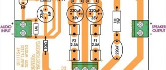
High fidelity amplifier Sukhov (VVS-2011)
Sukhov himself, in a recent video on YouTube, complained that the Radio printed a diagram with a gross error; the balancing pins were connected incorrectly. I was interested in something else, the reaction of the circuit to adding a capacitance in parallel with resistor R5. Yes it works. The signal front with it is noticeably more vertical. The rest is fine. Pre-weekend I took BD139 BD140, proven and chic in many ways. K553UD2 (153 UD2) - I agree, excellent sound design, with a tiny shift, very calm and predictable. I regret that at one time I did not collect them in stock, in metal and with acceptance. Riga made them. Even in the circuit for 1978, protection against excess current in the load was elegantly solved. I will definitely return to this scheme taking into account all your advice. OPA 627 there are a couple. Real ones. But in this scheme there is no need for high-speed opera. The same OPA 134 or 2134 dual are quite suitable. Their shift is tiny, due to the adjustment of resistors on the chip. There are also our K574UD2, dual ones, very good, although of average speed. ———- I know about the horse current through the pre-output transistors in the UMZCH BB, I also estimated the mode of the current sources. But there is some truth to this, in the circuit for 1978 there is no current at all, 5 mA. The performance is collapsing. We need something in between. Of all the things I've redesigned in recent years, but the circuit remains and works, it's a very simple AV device based on a high-speed operating system like 544UD2 and a couple of field-side laterals at the output, connected by a repeater. Operator with flying power, voltage boost from the outlet of its power supply into the ground, according to Ageev. The only condition for its normal operation in such a connection is that the impedances at both inputs of the microcircuit must be equalized in order to avoid distortions that arise when recharging the input capacitors. This is well described in an article by Ageev Radio 2 from 1987. Now this circuit is being used in a microphone station to test the speakers. Reliable, with clear beautiful sound and decent power. Yesterday I became convinced of the uselessness of additional repeaters that unload the op-amp; with them, the rate of rise of the pulse front decreases, and the fronts themselves become asymmetrical. The operator has enough current to distort the gates of the field workers. I measured the output stage itself, it runs without a block up to 3 MHz, then a smooth decline. When assembled, the amplifier operates on a full signal up to 300-400 kHz, on an average signal - a couple of volts - up to 1 MHz. Of course, these numbers are before connecting the protective RC circuit at the amplifier input. For those interested, my ULF named AB2 was made using the same scheme, on my author’s page. There are also links to the authors of this marvelous scheme. I don’t know anything simpler or better for myself, if we are talking about high-quality, uncomplicated and sufficiently powerful ULF without wild bells and whistles and the battle for hundreds of watts for dubbing a living space.
AMPOVIC ADULTOTHER VOLTAGE AMPLIFIERS
CHAMELEON
However, Lanzar's circuit design can be slightly changed, significantly improving the characteristics, increasing the efficiency without using an additional power source, if you pay attention to the weak points of the existing amplifier. First of all, the reason for the increase in distortion is the changing current flowing through the transistors, which varies over fairly large ranges. It has already been found out that the main signal amplification occurs in the last stage of the UNA, which is controlled by the transistor of the differential stage. The range of changes in the flowing current through the differential stage is quite large, since it needs to open the transistor of the last stage of the UN, and the presence of a non-linear element as a load (base-emitter junction) does not contribute to maintaining the current at a changing voltage. In addition, in the last stage of the UNA, the current also varies over a fairly wide range. One of the options for solving this problem is to introduce a current amplifier after the differential stage - a banal emitter follower, which unloads the differential stage and allows more precise control of the current flowing through the base of the last stage of the UNA. To stabilize the current, current generators are usually introduced through the last stage of the UNA, but this option will be postponed for now, since it makes sense to try a lighter option, which will also significantly affect the increase in efficiency. The idea is to use a voltage booster, not just for a separate cascade, but for the entire UA. One of the first options for implementing this concept was the power amplifier by A. Ageev, quite popular in the mid-80s, published in RADIO No. 8, 1982 (Figure 45, model AGEEV.CIR).
Figure 45
In this circuit, the voltage from the output of the amplifier is supplied, through a divider R6/R3, for the positive side and R6/R4 for the negative, to the power terminals of the operational amplifier used as a voltage amplifier. Moreover, the DC voltage level is stabilized by D1 and D2, but the magnitude of the variable component just depends on the amplitude of the output signal. Thus, it was possible to obtain a much larger amplitude at the output of the op-amp without exceeding the value of its maximum supply voltage, and it became possible to power the entire amplifier from +-30 V (this version was adapted for imported element base, the original source was powered from +-25 V, and the op-amp was with a maximum supply voltage of +-15 V). If you switch to the TRANSITION PROCESS STUDY
, then the following oscillograms will appear on the “oscilloscope screen”:
Figure 46
Here the blue line is the plus supply voltage, the red line is the minus supply voltage, the green line is the output voltage, the pink line is the positive supply voltage output of the op-amp, the black line is the negative supply voltage output of the op-amp. As can be seen from the “oscillograms,” the op-amp supply voltage remains at 18 V, but only relative to each other, and not relative to the common wire. This made it possible to increase the voltage at the output of the op-amp to such a value that even after two emitter followers it reaches 23 V. Based on the idea of floating power, which was used by Ageev, as well as by introducing a current amplifier after the differential stage, a power amplifier was designed, the circuit which is shown in Figure 47, model Chameleon_BIP.CIR, called Chameleon, because it allows you to adjust the main modes to the used supply voltage - adjusting the quiescent current of the last stage of the UNA.
Figure 47 ()
In addition to the circuit solutions described above, another one was introduced - regulation of the quiescent current of the last stage of the UNA, and with thermal stabilization elements. The quiescent current of the last stage of the UNA is adjusted by trimming resistor R12. On transistors Q3 and Q6, emitter followers are made that unload the differential stage; on the chains R20, C12, R24, R26 for the positive arm and on R21, C13, R25, R27 for the negative arm, a voltage boost for the UNA is made. In addition to increasing the efficiency, the voltage booster performs another secondary function - due to the fact that the actual amplitude of the signal has decreased, the range of changes in the current through the last stage of the VNA has also decreased, which made it possible to abandon the introduction of a current generator. As a result, the THD level at an input voltage of 0.75 V was:
Figure 49
As can be seen from the resulting graph, the THD level decreased almost 10 times compared to Lanzar with PBVC. And here your hands are already starting to itch - having such a low THD level, you want to increase your own gain, add more end-of-line transistors and “overclock” this amplifier to a pop level with an output power of about 1 kW. For experiments, you should open the file Chameleon_BIP_1kW.CIR and carry out a series of primary “measurements” - quiescent currents, the value of direct voltage at the output, frequency response, THD level. The obtained characteristics are impressive, but... It is at this point that practice interferes with theory, and not in the best way. To find out where the problem is hidden, you should run DC CALCULATION
and turn on the power dissipation display mode. You should pay attention to the transistors of the differential stage - about 90 mW is dissipated on each. For the TO-92 case, this means that the transistor begins to heat up its case, and given the fact that both transistors must be as close to each other as possible in order to warm up evenly and maintain equal quiescent currents. It turns out that the “neighbors” not only warm themselves, but also warm each other up. Just in case, it should be recalled that when heated, the current through the transistor increases, therefore, the quiescent current of the differential cascade will begin to increase and change the operating modes of the remaining cascades. For clarity, set the quiescent current of the final stage to 200 mA, and then assign a different name to transistors Q3 and Q6, right in the designation window, add a lower hyphen and a unit to get the following: 2N5410_1 and 2N5551_1. This is necessary to exclude the influence of variable parameters of the differential stage transistors. Next, you need to set the temperature of the differential stage transistors to be equal to, for example, 80 degrees. As can be seen from the resulting calculations, the quiescent current has decreased, and by so much that a “step” will already be observed. It is not difficult to calculate that with an initial quiescent current of 50 mA, the quiescent current of the final stage will become practically zero as the differential stage warms up, i.e. the amplifier will switch to class B. The conclusion suggests itself - it is necessary to reduce the power dissipation of the differential stage, but this can only be done by reducing the quiescent current of these transistors, or by lowering the supply voltage. The first will cause an increase in distortion, and the second will cause a decrease in power. There are two more options for solving the problem - you can use heat sinks for these transistors, but this method, despite its efficiency, does not add much to reliability - constant blowing of the case is required to prevent the radiators from heating up to critical temperatures in a poorly ventilated case. Or change the circuit design once again. However, before the next change, this amplifier still needs to be modified, namely, increase the ratings of R24 and R25 to 240 Ohms, which will entail a slight decrease in the supply voltage of the UNA, and of course, reduce the supply voltage to +-90 V, and slightly reduce its own gain .
Cooling the differential stage of the Chameleon amplifier of the previous version
As a result of these manipulations, it turns out that this amplifier with an input voltage of 1V is capable of developing about 900 W at a load of 4 Ohms, with a THD level of 0.012%, and with an input voltage of 0.75 V - 0.004%. For insurance, you can put pieces of tube from the telescopic antenna of the radio on the transistors of the differential stage. To do this, you need 6 pieces with a length of 15 mm and a diameter of 5 mm. Place thermal paste inside the tube, solder the tubes together, having previously placed them on the transistors of the differential stage and the emitter followers following them, and then connect them to the common one. After these operations, the amplifier turns out to be quite stable, but it is still better to use it with a supply voltage of +-80 V, since an increase in the mains voltage (if the power source is not stabilized) will lead to an increase in the power supply of the amplifier and there will be a margin for temperature conditions. Radiators for the differential cascade can not be used if the supply voltage does not exceed +-75 V. The printed circuit board drawing is in the archive, installation is also on 2 floors, performance testing and adjustment are the same as in the previous amplifier.
AMPLIFIER VP or STORM or?
Next, we will consider an amplifier better known as “V. PEREPELKIN’S AMPLIFIER” or “VP AMPLIFIER”, however, by putting OR in the title of the chapter there was in no way an intention to encroach on V. Perepelkin’s work on designing a series of his amplifiers - a lot of work was done and in In the end we turned out to be pretty good and versatile amplifiers. However, the circuitry used has been known for quite a long time and attacks on STORM regarding alteration and cloning are not entirely fair and further consideration of the circuitry solutions will provide comprehensive information about the design of both amplifiers. In the previous amplifier, a problem arose with the self-heating of the differential stage at high supply voltages and the maximum power that could be obtained using the proposed circuit design was indicated. The heating of the differential cascade itself can be eliminated, and one of the options for solving this problem is to divide the dissipated power into several elements, but the most popular is to include two transistors connected in series, one of them working as part of the differential cascade, the second is a voltage divider. Figure 60 shows diagrams using this principle:
Figure 60
In order to understand what happens with this solution, you should open the file WP2006.CIR, which is an amplifier model from V. Perepelkin, known on the Internet as WP. The amplifier uses a UN, built according to the principles of the above examples, but slightly modified - the output stage of the UN does not operate on a thermal stabilization transistor, as is usually the case, but is actually a separate device with one output - the connection point of the collectors of transistors Q11 and Q12 (Figure 61) .
Figure 61()
The circuit contains the actual ratings of one of the amplifiers, however, it was necessary to select a resistor R28 on the model, otherwise there would be an unacceptable constant voltage at the amplifier output. When checking DC CALCULATION
The thermal conditions of the differential cascade are quite acceptable - 20...26 mW is allocated to the differential cascade. The Q3 transistor installed above dissipates a little more than 80 mW, which is also within the normal range. As can be seen from the calculations, the introduction of transistors Q3 and Q4 is quite logical and the problem of self-heating of the differential stage is solved quite successfully. It should be noted here that Q3, like Q4, can dissipate a little more than 100 mW, since the heating of this transistor affects the change in the quiescent current only of the last stage of the NA. In addition, this transistor has a rather strict connection to the base current - for constant voltage it operates in emitter follower mode, and for the variable component it is a cascade with a common base. But the gain in alternating voltage is not large. The main burden of increasing the amplitude is still on the last stage of the NA and higher requirements are still placed on the parameters of the transistors used. The final stage uses a voltage booster organized on capacitors C16 and C17, which made it possible to significantly increase the efficiency. Taking into account the nuances of this amplifier and the desire to use a traditional output stage, the next model was created - Stormm AB.CIR. The schematic diagram is shown in Figure 62.
Figure 62 ()
To increase the efficiency, this amplifier uses a floating power supply for the UNA, an integrator on X2 is added to automatically maintain zero at the output, and an adjustment of the quiescent current (R59) of the last stage of the UNA is also introduced. All this made it possible to reduce the thermal power released on the transistors of the differential stage to the level of 18 mW. In this embodiment, overload protection of the Lynx-16 amplifier was used (it is assumed that Q23 controls the thyristor, which in turn controls the optocoupler connecting pins T4 and T5). In addition, the latest amplifier uses another not entirely traditional approach - high-capacity capacitors are installed in parallel with resistors R26 and R27, which made it possible to significantly increase the gain of this stage - it’s no secret that resistors in the emitter circuits are used for thermal stabilization and the more the value of this resistor, the more thermally stable the cascade will be, but the cascade gain will be proportionally reduced. Well, since this section is quite critical, capacitors C15 and C16 need to be used as capacitors that can recharge quickly enough. Conventional electrolytes (TK or SK) only introduce additional distortion due to their inertia, but capacitors used in computer technology, often referred to as pulsed (WL), cope perfectly with the tasks assigned to them (Figure 63).
Figure 63
All these changes made it possible to increase thermal stability, as well as quite seriously reduce the THD level (you can verify this, as well as check the degree of thermal stability yourself). The schematic diagram for the two-block version is shown in Figure 64, model Stormm_BIP.CIR
Figure 64 ()
The name STORM was given for the ability to painlessly increase the supply voltage to +-135, which in turn makes it possible, using separate switches, to transfer the amplifier to class G or H, and this is a power of up to 2000 W. Actually, the VP-2006 amplifier also translates well into these classes; more precisely, the progenitor was designed for class H, but since such high powers are practically not needed in everyday life, and the potential in this circuitry is quite good, the switches were removed and a pure class AB appeared .
HOLTON AMPLIFIER
The principle of dividing the dissipated power of a differential stage is also used in the fairly popular Holton amplifier, the circuit diagram of which is shown in Figure 65.
Figure 65 ()
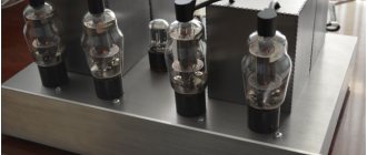
The amplifier model is in the file HOLTON_bip.CIR. It differs from the classic version in the use of bipolar transistors as the final stage, therefore it is strongly recommended to use field-effect transistors as the penultimate stage. The values of resistors R3, R5, R6, R7, R8 were also slightly adjusted, and the zener diode D3 was replaced with a higher voltage one. All these replacements are caused by the need to return the quiescent current of the differential stage to a level that ensures minimal distortion, as well as to more evenly distribute the dissipated power. When using an amplifier with a power supply less than that used in this model, it is necessary to select the indicated elements in such a way that the required quiescent current of the differential stage returns again. Circuit design features include a current generator in the differential cascade and symmetry of the input signal with respect to the feedback signal. When powering the UNA from a separate power source, you can achieve a truly maximum output power. The appearance of the finished amplifier (300 W version with bipolar output) is shown in Figures 66 and 67.
Figure 66
Figure 67
Next, several models of amplifiers are proposed, which to one degree or another do not differ in complex circuitry, but have good parameters.
ALMOST NATALY
This is a rather simplified version of the high-quality NATALY amplifier, however, the parameters of the simplified version turned out to be quite good. Model in file Nataly_BIP.CIR, circuit diagram in Figure 68.
Figure 68 ()
REMIX SUHOVA
Sukhov's remix because this is the same VV amplifier by N. Sukhov, only it is made according to a symmetrical circuit and uses completely imported equipment. Schematic diagram in Figure 69, model in the file Suhov_sim_BIP.CIR.
Figure 69 ()
I would like to dwell on this model in a little more detail, since it was embedded in metal (Figure 69-1).
Figure 69-1
Even with the naked eye you can see that the UN looks somewhat peculiar - there are parts soldered on top, the purpose of which is worth explaining. They are designed to calm this amplifier, which turned out to be very prone to agitation. By the way, it was not possible to completely calm him down. Stability appears only at a quiescent current of the final stage of the order of 150 mA. The sound is not bad at all, the dial THD meter, which has a limit of 0.1%, shows practically no signs of life, and the calculated values are also very indicative (Figure 69-2), but reality speaks of something completely different - either a serious reworking of the board is required, the boards in which most of the recommendations for board layout were followed, or this circuit design was abandoned.
Figure 69-2
Should I say that this amplifier was a failure? It is possible, of course it is possible, but THIS amplifier is an example of the fact that modeling is far from reality and a real amplifier can differ significantly from the model. Therefore, this amplifier is written off as a puzzle, and several more are added to it, which were used together with the same UN. The proposed options have a final cascade that works with its own OOS, i.e. having their own coffee shop. gain, which allows you to reduce the gain of the UA itself and, as a result, reduce the THD level.
Figure 69-3 Schematic diagram of an amplifier with a bipolar final stage ()
Figure 69-4 THD circuits of Figure 69-3
Figure 69-4 Circuit diagram with field output stage ()
Figure 69-6 THD circuits of Figure 69-5
VL BEST
Minor modifications, the introduction of a buffer amplifier based on a good op-amp with repeaters to increase the load capacity had a very good effect on the parameters of this amplifier, which was also equipped with a balanced input. Model VL_POL.CIR, circuit diagram in Figure 70. Models VL_bip.CIR - bipolar version and VL_komb.CIR - with field workers in the penultimate cascade.
Figure 70 ()
OM
Quite a popular amplifier, however, the model of the original version did not make an impression (file OM.CIR), so some changes were made when refining the UN for the proposed design. The results of the change can be viewed using the file with the OM_bip.CIR model; the schematic diagram is shown in Figure 71.
Figure 71 ()
TRANSISTORS
The models use transistors that may not be available everywhere, so it would not be fair not to supplement the article with a list of transistors that can be used in real amplifiers.
NAME, STRUCTURE
| U ke, V | I k, A | h 21 | F 1, MHz | P k,W | FRAME | ||
| NPN | PNP | ||||||
| BC546 | BC556 | 65 | 0.1 | <450 | 300 | 1 | TO-92 |
| 2SC3468 | 2SA1371 | 300 | 0.1 | <320 | 150 | 1 | TO-92 |
| MPSA42 | MPSA92 | 300 | 0.1 | >40 | 50 | 0.5 | TO-92 |
| 2N5551 | 2N5401 | 15 | 0.2 | <240 | 300 | 0.6 | TO-92 |
| KSE(MJE)340 | KSE(MJE)350 | 300 | 0.5 | <240 | ? | 20 | TO-126 |
| BD135,137,139 | BD136,138,140 | 45,60,80 | 1.5 | <250 | ? | 12 | TO-126 |
| 2SD669A | 2SB649A | 160 | 1.5 | <200 | 140 | 20 | TO-126 |
| 2SC5171 | 2SA1930 | 180 | 2 | <320 | 200 | 20 | TO-220 (formation) |
| 2SC3298B | 2SA1306B | 200 | 1.5 | <240 | 100 | 20 | TO-220 (formation) |
| 2SC4793 | 2SA1837 | 230 | 1 | <320 | 100 | 20 | TO-220 (formation) |
| MJE15032 | MJE15033 | 250 | 8 | >50 | 30 | 50 | TO-220 |
| MJL3281A | MJL1302A | 260 | 15 | <150 | 30 | 200 | TO-264 |
| 2SC3263 | 2SA1294 | 230 | 15 | >50 | 35 | 130 | TO3P |
| 2SC5359 | 2SA1987 | 230 | 15 | <160 | 30 | 180 | TO-264 |
| 2SC5200 | 2SA1943 | 230 | 15 | <160 | 30 | 150 | TO-264 |
| 2SC3281 | 2SA1302 | 200 | 15 | ? | 10 | 150 | TO-247 |
| 2SC3856 | 2SA1492 | 180 | 15 | <160 | 130 | TO3P | |
| 2SD1047 | 2SB817 | 140 | 12 | <200 | 100 | TO-247 | |
| 2SC3182 | 2SA1265 | 140 | 10 | <160 | 30 | 100 | TO-264 |
| N CHANNEL | P CHANNEL | ||||||
| IRF630 | IRF9630 | 200 | 6.5 | 74 | TO-220 | ||
| IRF640 | IRF9640 | 200 | 11 | 100 | TO-220 | ||
| IRFP240 | IRFP9240 | 200 | 12 | 150 | TO-247 | ||
| 2SK1530 | 2SJ201 | 200 | 12 | 150 | TO-264 |
With reference data, everything seems to be clear, however... The general race for profit causes problems not only at the level of retail trade in a market stall, but also in serious enterprises. The license for the release of IRFP240-IRFP920 was purchased by Vishay Siliconix Corporation and these transistors are already different from those that were previously produced I
international
rectifier
. The main difference is that even within the same batch the gain of the transistors varies quite significantly. Of course, it will not be possible to find out why the quality has decreased (deterioration of the technological process or rejection of the Russian market), so you have to use what you have and from THIS you need to choose what is suitable. Ideally, of course, you should check both the maximum voltage and maximum current, but the main parameter for the amplifier builder is the gain coefficient and it is especially important if several transistors connected in parallel are used. Of course, you can use the gain meter available in almost every digital multimeter, but there is only one problem - for medium and high power transistors, the gain strongly depends on the current flowing through the collector. In multimeters, the collector current in the transistor tester is a few milliamps and its use for medium and high power transistors is tantamount to guessing on coffee grounds.
It is for this reason that a stand was assembled for rejecting power transistors, not even for rejection, but for selection. The schematic diagram of the stand is shown in Figure 72, the appearance is shown in Figure 73. The stand is used for selecting transistors with the same gain
, but not for finding out the meaning of h21.
Figure 73
Figure 74
The stand was assembled within three hours and literally used what was lying in the “ANTIQUES” box, i.e. something that is not difficult to find even for a novice solderer. Indicator - level indicator of a reel-to-reel tape recorder, type M68502. The indicator was opened at the place where the top and bottom covers were glued, the standard scale was removed, and instead a scale was pasted on, which can be printed using a DOK document and contains reminders for switching operating modes. The sectors are filled in with colored markers. The indicator covers were then glued together using SUPERGLUE (Figure 75).
Figure 75
Toggle switches are essentially any toggle switches with two fixed positions, and one MUST have TWO switching groups. Diode bridge VD10 - any diode bridge with a maximum current of at least 2 A. Network transformer - any transformer with a power of at least 15 W and an alternating voltage of 16 ... with good area). C1 and C2 have a sufficiently large capacity, which guarantees that the needle does not shake during measurements. C1 for a voltage of 25 V, C2 for 35 or 50 V. Resistors R6 and R7 are pressed through a mica gasket to the radiator on which the KRENK is installed, generously coated with thermal paste and pressed with a strip of fiberglass using self-tapping screws. The most interesting is the design of the clamps for connecting the terminals of the transistors under study. To manufacture this connector, a strip of foil fiberglass was required, in which holes were drilled at a distance from the transistor output of the TO-247 case, and the foil was cut with a stationery cutter. Three knives from the SCART-MAMA television connector were sealed into the holes on the foil side. The knives were folded together, almost tightly (Figure 76).
Figure 76
The distance “L” is selected so that the housings of the TO-247 (IRFP240-IRFP9240) and TO-3 (2SA1943-2SC5200) transistors are placed on the fixing pin.
Figure 77
Using the stand is quite simple: When selecting field-effect transistors, the MOSFET
and the type of transistor is selected - with an N channel or a P channel.
Then the transistor is put on the pin, and its leads are applied to the contact blades of the connector. Then, using a variable resistor, let's call it CALIBRATION
, the arrow is set to the middle position (which will correspond to a current flowing through the transistor of 350-500 mA). Next, the transistor is removed and the next candidate for use in the amplifier is installed in its place and the position of the arrow is remembered. Next, the third candidate is installed. If the arrow deviates in the same way as on the first transistor, then the first and third can be considered basic and the transistors can be selected according to their gain coefficient. If the arrow on the third transistor deviates in the same way as on the second and their readings differ from the first, then recalibration is performed, i.e. resetting the arrow to the middle position and now the second and third transistors are considered basic, and the first is not suitable for this sorting batch. It should be noted that there are quite a lot of identical transistors in a batch, but there is a chance that recalibration may be required even after selecting a significant number of transistors.
Figure 78
Transistors of a different structure are selected in the same way, only by switching the right toggle switch to the P-CHANNEL
.
To test bipolar transistors, switch the left toggle switch to the BIPOLAR
(Figure 79).
Figure 79
Finally, it remains to add that having a stand in hand, it was impossible to resist checking the coffee amplification of Toshiba products (2SA1943 and 2SC5200). The result of the inspection is quite sad. Transistors for storage were grouped into four pieces of one batch, as the most convenient storage for personal use - amplifiers are mainly ordered for either 300 W (two pairs) or 600 W (four pairs). SEVEN (!) quadruples were tested and only in one quadruple of direct and in two quadruples of reverse transistors the gain was almost the same, i.e. After calibration, the arrow deviated from the middle by no more than 0.5 mm. In the remaining fours, there was always an instance with either a higher or lower gain coefficient and was no longer suitable for parallel connection (deviation by more than 1.5 mm). The transistors were purchased in February-March of this year, since the purchase of last year in November ended. The indication of deviations in mm is purely conditional, for ease of understanding. When using an indicator of the type indicated above, a resistance R3 equal to 0.5 Ohm (two 1 Ohm resistors in parallel) and the position of the indicator arrow in the middle, the collector current was 374 mA, and with a deviation of 2 mm it was 338 mA and 407 mA. Using simple arithmetic operations, we can calculate that the deviations of the flowing current are 374 - 338 = 36 in the first case and 407 - 374 = 33 in the second, and this is slightly less than 10%, which is no longer suitable for parallel connection of transistors.
PRINTED CIRCUIT BOARDS
Printed circuit boards are not available for all of the amplifiers mentioned, since processing printed circuit boards takes quite a lot of time + also assembly to check functionality and identify installation nuances. Therefore, below is a list of available boards in LAY format, which will be updated from time to time. Added printed circuit boards or new models can be downloaded either from the links that will supplement this page:
| PRINTED BOARDS IN LAY FORMAT | |
| MICRO-CAP 8 contains all the models mentioned in this article in the SHEMS , in addition, in the cv there are several examples of filters for building “color music”, in the EQ there are several filter models for building equalizers. | |
| Output stage board | |
| UN for assembly of UMZCH LANZAR | |
| UN for assembling UMZCH HOLTON | |
| UN for assembly REMISK SUKHOV (not stable) | |
Literature and almost literature: G.A. Kardashev, “Virtual electronics”, MRB, issue 1251 M.A. Amelina, S.A. Amelina “Circuit modeling program MICRO-CAP 8”, “Hot line-Telecom”, 2007 D.I. Ataev, V.A. Bolotnikov, “Practical schemes for high-quality sound reproduction” MRB, issue 1109 “SOLDERING IRON” Forum Vegalab Forum
Fans of MICROSIM who claim that it is much better, more convenient and more accurate than MICROCAP are better off reading the debate on this issue HERE and below.
A series of video tutorials on using MICROCAP was created:
BACK
Site administration address