We have noticed that the main disadvantage of an RC coupled amplifier is that the effective load resistance is reduced. This is because the input impedance of the amplifier is low and its output impedance is high.
When they are connected to create a multi-stage amplifier, the high output impedance of one stage goes in parallel with the low input impedance of the next stage. Consequently, the effective load resistance decreases. This problem can be solved using an amplifier
with
transformer connection
.
In a transformer amplifier, the amplifier stages are connected using a transformer. Let's look at the design and operational details of a transformer-coupled amplifier.
Construction of a transformer amplifier
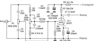
An amplifier circuit in which the previous stage is connected to the next stage using a coupling transformer is called transformer coupled amplifier.
The coupling transformer T 1 is used to feed the 1st stage output to the 2nd stage input. The collector load is replaced by the primary winding of the transformer. The secondary winding is connected between the potential divider and the base of the 2nd stage, which provides the input for the 2nd stage. Instead of a coupling capacitor as in an RC coupled amplifier, a transformer is used to couple any two stages in the amplifier circuit to the transformer.
The figure below shows the circuit diagram of a transformer coupled amplifier.
The potential divider network R 1 and R 2 and the resistor R e together form a bias and stabilization network. The emitter bypass capacitor C e offers a low reactance path for the signal. Resistor RL is used as load impedance. The input capacitor C, present at the initial stage of the amplifier, connects the alternating signal to the base of the transistor. Capacitor CC is a coupling capacitor that connects two stages and prevents DC interference between stages and controls the offset of the operating point.
Types of power amplifiers for matching transformers
The following devices appear here:
- Input. Their task is to match the output impedance of the input signal source with the cascade that follows.
- Interstage. The same resistance is matched, but from the previous cascade. In this case, the input resistance of the new stage occurs.
- Weekend. The indicated resistance is normalized, but the final stage is normalized with the resistance of its influence.
Input data is indicated by letters:
- T is the first component.
- VT – input signal for transistor devices.
- Development numbering.
Example: TVT-1 is an input transformer for transistor units with designation number 1.
Output CTs are designated as follows:
- component – T,
- OT (final version for transistor devices)
- ordinal development figure.
Example: TOT-4 – output CT for devices with transistors, development No. 4.
Intercascade views have the following designations:
- T,
- M,
- number – power indicator,
- development numbering.
Example - TM15 - 45. This is a miniature ST with cascades, 15 A power. Development No. 45.
There are also TOL output models. Here:
- T – transformer,
- O - final,
- L – lamp type.
They completely maintain the specified parameters in the spectrum from 300 to 10,000 Hz. Their operating powers are in the range of 0.1…6 V*A. The permissible unevenness of characteristics at maximum frequencies is a maximum of 2 dB. The highest distortion rate is 5%.
Transformer amplifier operation
When an AC signal is applied to the base input of the first transistor, it is amplified by the transistor and appears at the collector to which the primary winding of the transformer is connected.
The transformer that is used as the connecting device in this circuit has the property of changing impedance, which means that a low stage (or load) resistance can be reflected as a high load resistance compared to the previous stage. Therefore, the voltage across the primary winding is transmitted according to the turns ratio of the secondary winding of the transformer.
This transformer coupling provides good impedance matching between the amplifier stages. A transformer coupled amplifier is typically used for power amplification.
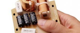
Calculation and winding of the output transformer for a tube amplifier
We select an output lamp - we build a load straight line and select the RT on the current-voltage characteristics, find the reduced resistance, select the acoustic (load) resistance, as a result we calculate the ratio of the turns of the primary and secondary windings = Ktr = √KV (reduced anode resistance: acoustic resistance).
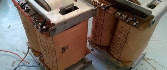
We choose a transformer - more iron, less copper, without fanaticism with overall power (from the practice of reproducing low frequencies), 100-160 W (10-14 cm2 of the central core area) is enough. It’s a paradox, the best sound comes from hardware from Chinese computer uninterruptible power supplies. TSSh-170 showed good results, although it has some inconveniences with assembly and fastening.
We stock up on a large tube of Moment glue, thin stationery tape and narrow masking tape. Caliper, metal precision ruler, calculator, pencil. MEASUREMENTS - a window that limits the iron, exactly to tenths of mm.
On the table is a table of the nominal diameters of the winding wire, cross-sections for copper and varnish, permissible current at current load.
We prepare the coil frame - we clean it from burrs, think about it, and then drill the required number of “holes” for the wire leads and contacts for soldering and fastening. If it doesn’t work out with the brains, we saw through a gap, one or two.
Holes for leads for fluoroplastic wire so that the thin winding wire does not break. The holes for fastening-soldering for bare copper are 0.75-1.0 mm, then we will tin them.
We are preparing intersectional insulation - strips of office paper with fringe 1.5 mm wider than the coil window on each side.
We measure:
Example: 34.5x10 mm, bottom = 34.5 mm, height = 10 mm.
Sectioning - connection of windings ONLY SERIES! Any layer is filled only completely and without gaps.
First, at least half of the primary , then intersectional insulation - 3 layers of prepared office paper with fringe, then a layer of secondary, intersectional insulation, then a quarter of the primary, intersectional 3 layers, a layer of secondary, intersectional, the remaining quarter of the primary, intersectional 3 layers, then you can layer primary (about 200 turns) for the cathode winding, and the last remaining layer of the secondary - it is advisable to make loop conclusions on it every 5-7 turns to adjust to specific acoustics, by ear.
The total is: ½ I – II – ¼ I – II – ¼ I – K – II (5+5+5+5+5+5)
CALCULATION
Let's estimate - the number of turns of the secondary in one layer of wire is about 1.0 for copper (from practice) - 1.09 lac.
34.5: 1.09 = 31.65 – 1 turn = 30 turns secondary layer.
There will be 3 (three) such layers.
My task is a 5k primary and two outputs at 8 Ohms and 16 Ohms.
We calculate the turns of the primary. Through Ktr, for 8 Ohms = 25, for 16 Ohms = 17.
(Ktr = square root [5k : Ra]) = root (5000 : = root 625 = 25 for 8 Ohms, and accordingly 16 Ohms = 17.
This means two layers of secondary – 8 Ohms, three layers – 16 Ohms.
Let's estimate the equality of the primaries.
Two layers of secondary = 60 turns (at 8 ohms) x 25 (Ctr 8 ohms) = 1500 turns - approximate primary at 8 ohms.
Three layers of secondary = 90 turns (at 16 Ohms) x 17 (Ktr 16 Ohms) = 1530 turns - almost the same. We choose the average (forgive the Internet GURU) = total primary 1515 turns.
Calculation of primary diameter
Actual window area = 34.5 x 10 = 345 mm2.
From practice , the primary and secondary require the same areas, for the primary = 345: 2 = 172.5 mm2.
From practice for swelling and insulation, we divide this area by 1.4 and get purely for the primary wire = 172.5: 1.4 = 123.21 mm2, divide it by the number of turns and get the area for one turn = 123.21 mm2: 1515 turns = 0.08133 mm2. We take the square root and get the required diameter of the primary wire over the varnish: √0.08133 = 0.2852 mm.
According to the table for varnish, we look for the nearest smaller one, it turns out for copper: 0.25 - 0.23 mm.
Because a 0.23 copper wire “holds” at least 110 mA = that’s enough for us, so we use it.
TOTAL: winding card = 758 (1515:2) turns 0.23 mm - insulation - 30 turns 1 mm - insulation - 379 (1515:4) turns 0.23 mm - insulation - 30 turns - insulation - 379 turns 0.23 mm – insulation – layer 0.23 mm – insulation – 30 (5+5+5+5+5+5) 1.
Let's rewind:
At the beginning and at the end of any layer we put a little glue so that the wire does not “microphone” and strengthens the paper.
Frisky - “we lay the long windings neatly in piles at a quarter height, fill the layer”
For very long windings, it is possible to use interlayer stationery tape in one layer.
It is advisable to mark the terminals of a thin winding wire with multi-colored cambrics:
We collect
Pushpul = without clearance, single stroke = with clearance.
With an anode current of up to 50 mA - a gap of 0.05 mm - one layer of tracing paper, with a current of 100-120 mA = a gap of 0.1 mm - one layer of ordinary office paper, ONLY ON THE CENTRAL CORE!
the leads of the thick wires and form them as connection terminals; there is no need to invent anything. Thin ones - we clean them by firing and carefully clean them with fine sandpaper. We tin it and securely solder it to a prepared PCB panel with about 1 mm terminals attached to bare wires. For convenience, we attach this socket with bolts in the closest place to the terminals from the coil.
Don’t forget the markings - on the “belly” of the coil, on the convenient side, under the adhesive tape, we glue a label for the winding card and the location of the contacts.
There is little left to do, we calculate the amplifier (a little later), we take out the lamp parts, we “mechanize” the case, we remove the power supply, we install, we burn rosin, we swear at the inconsistency of the Internet’s signed I-V curves, we recalculate to real measurements, we burn rosin, we replace knocked-out apartment plugs , we spit on the acoustics, and enjoy Waters, or the sound of “Blade Runner” (Shonochka is simply beautiful!).
Answers to the questions “Why?” We are looking in primary sources and God forbid we listen to Internet GoreGurus (and there are also those with a sanghi education), only through discharging 450 V capacitors on our own fingers = there is no other way!
Author: Yuri E.
Transformer-coupled amplifier frequency response
The figure below shows the frequency response of a transformer coupled amplifier. The amplifier gain is constant only over a small frequency range. The output voltage is equal to the collector current multiplied by the reactance of the primary winding.
At low frequencies, the reactance of the primary begins to drop, resulting in a decrease in gain. At high frequencies, the capacitance between the turns of the windings acts as a bypass capacitor to reduce the output voltage and hence the gain.
So the amplification of audio signals will not be proportional and some distortion will also be introduced which is called frequency distortion
.
Disadvantages of a transformer coupled amplifier
The following are the disadvantages of a transformer coupled amplifier.
- Although the gain is large, it varies significantly with frequency. Hence the poor frequency response.
- The distortion frequency is higher.
- Transformers tend to make a hum.
- Transformers are bulky and expensive.
Although the gain is large, it varies significantly with frequency. Hence the poor frequency response.
The distortion frequency is higher.
Transformers tend to make a hum.
Transformers are bulky and expensive.