Germanium above all? Long live experimentation!
The proposed stereo audio power amplifier (UMPA) is made using circuit design more than half a century old with one voltage amplification stage. Its distinctive feature is the use of “sound” silicon transistors.
Among lovers of high-quality sound reproduction, a similar structure based on germanium transistors is still popular [1-4]. And the high quality of sound reproduction of these amplifiers is explained by the “wonderful properties” of germanium. By comparing two designs with a similar circuit diagram, made on different element bases, you can verify in practice whether this is so.
Looking ahead, I will say that in the end we got three decent amplifiers. Both silicon and germanium are good with the right circuit design. Happy creativity!
Contents
- 1 Germanium is playing! 1.1 Ways to improve the known scheme
- 1.2 Schematic diagram of a modified UMZCH on germanium transistors
- 1.3 Characteristics of the modified amplifier
- 1.4 Recommended power supply
- 2.1 Amplifier circuit of a similar structure, but on silicon
↑ Germanium is playing!
Currently, germanium transistors are almost completely replaced by silicon ones, which have better parameters and, most importantly, better temperature stability.
The decisive reason for replacing germanium transistors with silicon ones was the higher cost and shortage of raw materials. Nevertheless, there are many germanium transistors left in the arsenals of radio amateurs, so it doesn’t hurt to once again evaluate the audio properties of germanium from a modern perspective.
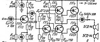
Let's consider an amplifier based on germanium transistors, built according to the circuit shown in Fig. 1. The amplifier is implemented in hardware by J. Tsikhiselli, published in the AudioVideo magazine [3]. The editorial specialists highly appreciated the sound of the amplifier.
Fragment excluded. The full version is available to patrons and full members of the community.
Rice. 1. Popular UMZCH circuit on germanium transistors
The proposed circuit is a direct-coupled DC amplifier. The preliminary stage on transistor VT1 amplifies the voltage signal and operates in class A. The output stage is a power amplifier operating in class AB with a small quiescent current. It is made on powerful transistors VT4, VT5 of the same conductivity type. The cascade on complementary transistors VT2, VT3 plays the role of a bass reflex. The output stage with a bass reflex can be represented as a quasi-complementary structure. The upper arm (transistors VT2, VT4) is a composite emitter follower - a Darlington circuit, and the lower arm (transistors VT3, VT5) is an amplifier with tracking feedback, otherwise called a Sziklai circuit.
Transistors VT2, VT4 amplify the negative half-wave of the signal voltage, and VT3, VT5 – the positive half-wave.
The disadvantage of the quasi-complementary structure of the output stage is the difference in the transmission coefficients for the upper and lower arms. The transmission coefficient of the lower arm is slightly higher than that of the upper arm, although their values are very close to unity.
The input impedances of the arms also differ, by approximately 4–8%; the upper arm has a higher input impedance than the lower arm (see Table 1).
The noted factors naturally determine the initial level of distortion of the amplifier, before being covered by negative feedback.
To obtain the maximum possible range of the output signal, positive feedback (POS) is applied, introduced by capacitor C2 from the output of the amplifier to the connection point of load resistors R4 and R5, increasing the equivalent load resistance for the variable component.
The voltage gain of the cascade on transistor VT1 determines the gain of the UMZCH without feedback:
Ku=h21e (Rn~||Rin)/rbe1=820 (58 dB),
where h21e is the base current transfer coefficient of transistor VT1, rbe1 is the resistance of the base-emitter junction of transistor VT1, Rн~ is the load resistance of VT1 taking into account the action of the PIC, Rin is the input resistance of the final stage.
The nonlinear nature of the base-emitter resistance of transistor VT1 also contributes to the initial level of amplifier distortion. Its significance can be reduced by using a pre-amplifier with a high output impedance or connecting a resistor in series with capacitor C1 to stabilize the input impedance of the cascade on transistor VT1.
Calculations show that, taking into account the above factors, the amplifier's harmonic distortion will be at the level of 0.1...0.2%.
Additional temperature stabilization of the operating point of transistor VT1 is achieved by introducing local negative DC feedback by including resistor R6 in the emitter circuit of VT1. For alternating current, the negative feedback is removed by shunting the specified resistor with capacitor C4.
In addition, increasing temperature stability is achieved by using resistance R3 in the base circuit VT1, as well as through resistors R8 and R9 in the emitter circuits VT2, VT3, designed to limit the reverse uncontrolled current of their collectors. General parallel DC feedback and midpoint potential adjustment is provided by trimming resistor R2.
Additional parallel OOS is provided by the chain R12, C5 located behind the transition capacitor C7, which ensures a wide frequency band, low output resistance and low distortion of the output signal.
Particular mention should be made of capacitor C5, which prevents possible unstable operation of the amplifier. The fact is that with the chosen method of adjusting the signal level at the input of the UMZCH, depending on the position of the variable resistor R1 slider, the depth of the feedback changes and, accordingly, the feedback transmission coefficient: Kuos = – (R2||R12)/R1,
where R1 is the resistance between the variable resistor motor and the UMZCH input.
The capacitance of the correction capacitor C5 is not taken into account here.
As a result, we may encounter unstable operation (generation) of the amplifier as the feedback depth increases, i.e. reducing the gain using variable resistor R1. The probability of excitation increases when the load (speaker system) is disconnected.
To explain this, consider the equivalent circuit of an amplifier (Fig. 2).
Rice. 2. Equivalent circuit of an amplifier with parallel voltage feedback
If Ku is large, the cascade is a current-to-voltage converter: Uout=–iinRoc.
To control the circuit from a voltage source Uin in Fig. Figure 2 shows the coupling capacitor Cvx and the resistor Ri, which determines the input resistance of the amplifier.
Due to the presence of input parasitic capacitance Cn, which is difficult to take into account, at high frequencies the circuit is a second-order link with a damping decrement depending on Cn and other factors.
The resulting amplitude-frequency response (AFC) has a rise at frequency 1/(2ΠTo) (Fig. 3).
Rice. 3. Possible logarithmic frequency response of the circuit
As a result, the circuit easily loses stability and goes into a state of self-oscillations, which are not constant, but unpredictable, depending on many factors. Minor fast influences, for example, interference in power circuits, abrupt changes in amplitude at a certain frequency, cause long-term, slowly decaying oscillations at a frequency of 1/(2ΠTo).
To obtain an even frequency response in the passband, it is enough to ensure that the mutual slope of the frequency response of the amplifier with feedback and the frequency response of the open-loop amplifier does not exceed 20 dB per decade.
An even frequency response can be obtained by turning on the capacitor Coc, its capacitance is selected from the ratio CocRoc=RiCp, while the feedback transmission coefficient becomes frequency-independent and equal to Ri/(Roc+Ri), and the bandwidth at high frequencies is determined by the above time constants Tp = CocRoc=RiCp.
One of the convenient and visual ways to monitor the frequency response of amplifiers is to check using rectangular pulses, Fig. 4. You can immediately see the presence of resonant frequencies and evaluate the bandwidth of the amplifier.
Rice. 4. Amplifier control using square pulses
The duration of the front τ f at a level of 0.9 characterizes the upper frequency:
fв=2.3/2πτ f=0.366/τ f, and the decay of the top of the pulse ∆ Usp – the lower frequency:
fн=ln (Uout/(Uout-∆ Usp))/2π tи=∆ Usp/2π tи Uout,
where ti is the pulse duration, Uout is the pulse amplitude.
Curve 1 in Fig. 4 shows the transient process caused by the instability of the amplifier.
Observing the response of the amplifier on an oscilloscope, we gradually increase Cos until the oscillations disappear and the transient process looks like curve 2.
Let me draw your attention to the fact that the establishment time of the pulse of a stable circuit turns out to be many times less than the transition process of curve 1
.
So, capacitor Cos (C5 in the circuit of Fig. 1) serves to ensure the “smoothness” of transient processes and the stability of the circuit
.
In order to guarantee the formation of the frequency response of cascades covered by negative feedback as a characteristic of an aperiodic (inertial) first-order link, another capacitor is introduced into the circuit - C3.
His task is to obtain such a characteristic of the loop amplification so that it has an aperiodic character.
Now, with abrupt changes in the input voltage at any frequency, the output voltage changes smoothly according to an exponential law, without surges or fluctuations.
The feedback bandwidth is approximately equal to
foc=(Ku/Kuoc)/(2π Rvt1effС3),
where Rvt1eff is the effective load in the collector circuit of transistor VT1, taking into account the action of the PIC.
In this case, the poles of transistors VT2-VT5 of the amplifier must lie below the Kuoc line. Considering that the frequency limit of the applied transistors VT2, VT3 is only 1 MHz, and that of the transistors VT4, VT5 of the output stage is even less - 0.2 MHz, in the circuit it is difficult to obtain foc of the order of 70...100 kHz.
To ensure stable operation of the amplifier with any load, including without it, it is recommended to include a Zobel circuit at the output, which loads the circuit in a wide frequency range. It seems that its absence is a consequence of ignorance of this circuit technique at the time of development of the circuit.
To eliminate step-type distortions, a small bias is applied to the bases of the output stage transistors VT2, VT4 and VT3, VT5, created by the flow of collector current VT1 through germanium diodes VD1, VD2.
The required output stage current (40 - 50 mA) is set by selecting the value of resistor R13, which shunts diode VD2.
For reliable operation of the amplifier in the temperature range 0...+50°C, diodes VD1, VD2 must have thermal contact with the radiator of one of the output transistors VT4, VT5. The cooling area of the heat sinks is at least 200 sq. cm.
Circuit R7, C6 is a filter for supplying the voltage amplification stage.
↑ Ways to improve the known scheme
Considering the above, I will draw attention to three points that can improve the sound quality, reliability and repeatability of the circuit shown in Fig. 1:
1. Select a constant voltage gain of the UMZCH by connecting a resistor in series with capacitor C1, and connect the amplifier itself to a low-impedance signal source. For the sensitivity of the UMZCH from the input Uin = 0.775 V, you should take a resistor with a resistance of 620 Ohms.
2. Ensure guaranteed stability of the amplifier by connecting in parallel with the output a stabilizing serial RC circuit: a 20 Ohm resistor and a 0.047 µF polypropylene, polystyrene or polyethylene terephthalate film capacitor (Zobel circuit).
3. Reduce the supply voltage to 30 V or less, since the selected element base does not ensure reliable operation of the amplifier at a supply voltage Up = 40 V.
↑ Schematic diagram of a modified UMZCH on germanium transistors
The schematic diagram of the UMZCH on germanium transistors, which I repeated, is shown in Fig.
5. Fragment excluded. The full version is available to patrons and full members of the community.
Rice. 5. UMZCH circuit on germanium transistors with implemented modifications
To eliminate radio frequency interference, inductance L1 is installed at the input in the form of a ferrite bead with a conductor passed through it.
Parallel negative feedback circuits for direct and alternating currents (R2, R3) and alternating current (R14, C6) are separated. This eliminates the influence of connecting the load (speaker system) on the DC operating mode of the UMZCH.
The trimming resistor R2 “Balance” sets half the voltage of the power supply at the point of symmetry, and the trimming resistor R9 “Quiet current” sets the initial current of the output stage transistors VT4, VT5. It is convenient to control the current value by the voltage drop across one of the resistors R12 or R13 in the emitter circuit of transistors VT4, VT5.
The oxide capacitors at the output of amplifier C7 and along the power supply circuit C10 are shunted by film capacitors C8 and C11, respectively.
At the output of the UMZCH, the Zobel circuit C9, R15 is connected.
Transistors for the amplifier are selected in pairs not only for the upper and lower arms of the output stage, but also for both channels. A transmission coefficient h21e of transistors of at least 100 is highly desirable. Transistors with the highest h21e are placed in place of VT1.
↑ Characteristics of the modified amplifier
Characteristics of UMZCH on germanium transistors with modifications:
Supply voltage: 30 V; Maximum power with a load resistance of 4 Ohms: 20 W; Current consumption at maximum power, no more than: 1.0 A; Frequency range: 20 Hz…20 kHz (–1.5 dB); Harmonic distortion at 18 W output power: 0.12%; Voltage gain: 12.4 (21.8 dB); Sensitivity: 775 mV; Output resistance, no more than: 0.5 Ohm.
↑ Recommended power supply
In Fig.
Figure 6 shows a variant of the power supply for the amplifier. A power transformer was used with a voltage on the secondary winding of ~22.5 V and a current of 2.2 A. The fragment was excluded. The full version is available to patrons and full members of the community.
Rice. 6. Recommended power supply circuit
Diode bridge KBPC1001 (100V/10A) can be replaced with BR1001. Capacitors C1...C4 type K73-17 for an operating voltage of 630 V, C5 - imported for a voltage of 50 V or more. Film capacitor C6 K73-17 for a voltage of 63 V. Resistor R1 of any type with a power of 0.5 W. LED HL1 - any green color, for example, AL307VM, AL307GM.
The power supply designed for the amplifier shown in Fig. 1, differs in the element base. Instead of the VD1 diode bridge, four D305 germanium diodes are installed; instead of film capacitors (C1 - C4, C6) - mica KSO, and oxide C5 consists of eight capacitors of the K50-29 or Philips type connected in parallel with a capacity of 1000 μF for an operating voltage of 63 V.
↑ High-power amplifier circuit
This is what my final amplifier circuit looks like. Changed denominations are indicated in red.
Not a single lawyer has yet been able to circumvent the Ohm and Joule-Lenz laws, and in order to increase the output power of the UMZCH, it is necessary to increase its supply voltage. Let's do it at least twice, up to 30 Volts. You won't be able to do this right away. Transistors P416 and MP39B, which are used in the original circuit, have a maximum permissible voltage of 15 Volts.
I had to take the old 1978 edition of the Amateur Radio Handbook off the shelf and delve into the study of the parameters of germanium transistors of the MP and GT series, while simultaneously excavating the boxes with parts.
I was looking for transistors with parameters close to those used in the circuit, but with a maximum permissible voltage of at least 30 Volts.
After carrying out this exciting research work, the necessary candidates were found. For the input, instead of P416, the main contender was the GT321D transistor. It was decided to replace the MP39B + MP37A pair with a similar MP14A + MP10B pair. Germanium transistors of the MP series with numbers from 9 to 16 are “military equipment”, transistors for special-purpose equipment. In contrast to their analogues with numbers from 35 to 42, which are intended for equipment of wide application.
At the output, I decided to use high-frequency GT906A transistors. There were several reasons for this, the main one being the presence of a supply of these transistors in my bedside table. The second reason is the high current transfer coefficient. During operation, the transistors of the preliminary stage will “strain” less to drive the output transistors, which should reduce their heating and have a positive effect on the level of distortion of the amplifier.
The next step, which is also important, is the selection of transistors in pairs according to the current transfer coefficient h21e. At first I tried to do this using a regular Chinese tester, but the measurement results seemed somewhat strange and clearly overestimated. In addition, the Chinese tester clearly could not cope with measuring the parameters of powerful transistors.
I had to take out the good old Soviet-era PPT device from the shelf.
With its help, a pair of GT321D transistors with h21e = 120 and two pairs MP10B + MP14A with h21e about 40 were selected. From a dozen 1T906A transistors, we managed to select 3 pcs. with beta 76 and a couple with beta 78. Still, the 1T series went through a more serious selection for parameters during manufacturing.
After selecting the transistors, assembling the printed circuit boards according to the Datagor instructions did not take much time. We also need to pay attention to the voltage of electrolytic capacitors. It must be no less than the selected amplifier supply voltage. I used 35 volt capacitors.
Since I planned to get more power from the amplifier, it was necessary to increase the capacity of the output coupling capacitor by at least two times. A capacitor of this rating could no longer fit on the board. Instead, I soldered a couple of screw terminals so that I could connect any capacitor I liked on the wires, regardless of its size.
Another important problem was the organization of cooling of the output transistors. I found a pair of identical, rather large radiators, but they were designed to accommodate modern transistors in the TO-220 housing. I found a solution in old burnt computer power supplies. A pair of radiators made of thick 4 mm aluminum, onto which I attached GT906 transistors through insulating gaskets, and these radiators themselves, with a wide end, were screwed through thermal paste to large radiators.
The amplifier boards were also attached to the same radiators using metal corners. Between the fins of the computer heatsink, near the output transistors, a D310 diode is conveniently placed, which ensures the thermal stability of the amplifier. Without hesitation, I filled it with Chinese hot melt glue.
↑ And now silicon sings!
Now let's analyze the circuit (Fig. 7), consisting of a voltage amplifier according to a circuit with a common emitter on transistor VT1 and a current amplifier on complementary composite emitter followers VT2, VT3.
↑ Amplifier circuit of a similar structure, but on silicon
Fragment excluded. The full version is available to patrons and full members of the community.
Rice. 7. Schematic diagram of a simple UMZCH on silicon transistors
The input signal is supplied to the base of transistor VT1 through decoupling capacitor C1, ferrite bead L1 and resistor R1.
The transmission coefficient of an amplifier covered by negative feedback (NFB) is determined by the divider R1, R7, R9, R10:
Ku= – [(R7+R10)||R9]/R1=– 11.5 (21.2 dB).
The constant resistor R7 and the tuning resistor R10 determine the DC operating mode of the circuit (voltage at the midpoint), and the resistor R9 is placed behind the transition capacitor C5, which linearizes its characteristic. As a result, the right (according to the circuit diagram in Fig. 7) terminal of resistor R9 is connected directly to the speaker system.
To ensure that when the loudspeaker is disconnected, the DC operating mode of the circuit does not change, resistor R13 is introduced. It performs another function in the circuit - it prevents clicks when connecting the speaker system. The output coupling capacitor results in a reduction in output power at low frequencies, as well as a deterioration in the damping factor.
With the capacitance of the coupling capacitor C6=4700 μF, load resistance Rн=4 (8) Ohm and lower frequency fн=20 Hz, the output power will decrease by {Rн/SQRT[(Rн^2+(Sπ fнС5)^2]}^2 times At a frequency of 20 Hz at Rн=4 Ohm, the output power will decrease by 15%, and at Rн=8 Ohm - by 4%.
Increasing the damping factor and output power at low frequencies is achieved using an additional feedback circuit through resistor R9.
The choice of sufficiently low resistance resistor values contributes to the stability of the OOS circuit throughout the entire audio range.
Resistors R6, R8 in the Darlington base circuits VT2, VT3 serve to prevent self-excitation of the emitter followers at high frequencies.
Elements R3, R4 and C4 form a “voltage boost” circuit, a PIC circuit to provide the required base current VT2 and VT3 at signal peaks and improve the quality of the negative half-wave of the output voltage.
The depth of the PIC through capacitor C4 is determined by the ratio of R4 to R3, as well as by the resistance value of resistors R11, R12 in the emitter circuits of transistors VT2, VT3.
Elements R2, VD1 – VD3 serve to provide initial bias in the base circuits of repeaters VT2, VT3. To ensure the temperature stability of the amplifier, good thermal contact of the diodes VD1 - VD3 with the radiators of the output transistors VT2, VT3 is necessary.
Using trimmer resistor R2, the quiescent current of the output stage is set in the range of 40 - 70 mA, the recommended value is 60 mA. It is set by the voltage drop across resistors R11, R12 (12 mV).
↑ Silicon amplifier details
Transistor VT1 type 2N5551 can be replaced with MPSA42, MPSA43.
It is advisable to select transistors with a transmission coefficient h21e=150...250. Complementary transistors 2SD2390/2SB1560 (Uke=150 V, Pk=100 W, Ik=10 A, fT=55 MHz, h21e=5000) in the TO-3R package, can be replaced with 2SD2438/2SB1587, 2SD2439/2SB1588 in the same case, as well as on 2SD2589/2SB1659 in the MT-200 case.
Power transistors VT2, VT3 are installed through heat-conducting substrates on a common radiator with a cooling surface area of at least 300 square meters. cm.
Capacitor C3 is ceramic for an operating voltage of at least 50 V; High voltage ceramics are acceptable. Inductance L1 in the form of a ferrite bead is soldered from faulty computer sound cards.
Many parts for this design can be ordered from the Datagorsk online store “Radio Components - By Mail!”
↑ Details of the amplifier for two channels
VT1 – Transistor 2N5551 – 2 pcs., VT2 – Transistor 2SD2390 – 2 pcs., VT3 – Transistor 2SB1560 – 2 pcs., VD1…VD3 – Diode 1N4148 – 6 pcs., R1 – Res. 0.25 -510 Ohm (blue , red, brown, golden) – 2 pcs., R2 – Res.adjustment.
300 Ohm Trim 3296W-1-301 – 2 pcs., R3 – Res.-0.25-200 Ohm (red, black, brown, gold) – 2 pcs., R4 – Res.-0.25-1.8 kOhm (brown, gray, red, golden) – 2 pcs., R5 – Res.-0.25-150 Ohm (brown, green, brown, golden) – 2 pcs., R6, R8 – Res.-0.25 -68 Ohm (blue, gray, black, gold) – 4 pcs., R7 – Res.-0.25-33 kOhm (orange, orange, orange, gold) – 2 pcs., R9 – Res.-0.25 -9.1 kOhm (white, brown, red, gold) – 2 pcs., R10 – Res. trim. 33 kOhm Trim 3296W-1-333 – 2 pcs., R11, R12 — Res.-5-0.1 Ohm SQP – 4 pcs., R13 – Res.-1-470 Ohm (yellow, purple, brown, gold) – 2 pcs., R14 – Res.-0.5-20 Ohm (red, black, black, gold) – 2 pcs., C1 – Cond. 220/25V 0812 +105°C– 2 pcs., C2 – Cond. 470/16V 1013 +105°С – 2 pcs., C3 – Cond. NPO 33 pF 5% ceramic. imp. – 2 pcs., C4 – Cond. 100/63V 1013 +105°C – 2 pcs., C5 – Cond. 4700/50V 2235+105°С – 2 pcs., C6 – Cond. 1/63V K73-17 – 2 pcs., C7 – Cond. 470/63V 1321 105°C – 2 pcs., C8 – Cond. 0.047/630V K73-17 – 2 pcs., C9 – Cond. 0.68/63V K73-17 – 2 pcs., L1 – Inductance Ferrite beads – 2 pcs., X1, X2 – Terminal block 2K pitch 5 mm on TV-01A board – 2 pcs., X3…X6 – Knife terminal on the board TA-M/DJ610-6.3 – 8 pcs., 2A2318 – Heat-conducting substrate for TO-218, TO-247, with hole. – 4 pcs., Printed circuit board 70x85 mm – 2 pcs. The details of each UMZCH channel are located on a separate printed circuit board, Fig. 8.
Rice. 8. Placement of parts of one UMZCH channel
The appearance of the assembled printed circuit board of one UMZCH channel is shown in the abstract of the article.
The UMZCH connection in the device is made with a wire with a cross-section of 0.75 - 1 sq. mm. The mating part for the wires are 6.3 mm knife terminals (preferably insulated), designed for the specified wire cross-section. Crimping of knife terminals is performed with a special tool (Fig. 9). Pliers or a hammer will not provide the quality of connection achieved with special tools.
Rice. 9. Pliers for crimping terminals and contacts onto wires
↑ Setting up the amplifier
begin after carefully checking the correct installation.
Particular attention is paid to the correct installation of transistors, oxide capacitors and diodes, as well as the quality of soldering. To simplify setup, the slider of the trimming resistor R2 is set to the minimum resistance position, and the slider of the resistor R10 is set to half the nominal value. When turned on for the first time, the input jacks X1, X2 must be short-circuited and an equivalent load must be connected to the output. Operating modes should not differ from those indicated on the circuit diagram by more than 10%.
After a twenty-minute warm-up, resistor R10 sets the voltage at the symmetry point equal to half the supply voltage, and resistor R2 sets the output stage current to 60 mA, based on the voltage drop across resistors R11, R12 equal to 12 mV.
↑ Characteristics of its silicon counterpart
If instrumentation is available, the characteristics of the UMZCH are taken.
Characteristics of a simple UMZCH:
Supply voltage: 30 V; Maximum power with a load resistance of 4 Ohms: 20 W; Current consumption at maximum power, no more than: 1.0 A; Frequency range: 20 Hz…20 kHz (–0.5 dB); Harmonic distortion at 18 W output power: 0.03%; Voltage gain: 11.5 (21.2 dB); Sensitivity: 775 mV; Output resistance, no more than: 0.025 Ohm.
When connecting the amplifier to the sound reproduction path, it should be taken into account that it is inverting. It is necessary to take measures so that the path as a whole maintains the phase of the signal, i.e. was non-inverting. For example, take this fact into account by changing the polarity of connecting the speaker wires. However, the DACs of some players (for example, Pioneer BDP-170) invert the phase of the input signal, which, however, is not reflected in any way in the user manual.
↑ Some measurements
After setting the DC modes, I connected a generator and an oscilloscope to the amplifier. He gave a signal.
output , signal limitation (blue color) occurs at an amplitude of approximately 12 Volts at a 4-ohm load, and this corresponds to an output power of 18 W. Hooray!!! :yahoo: The signal amplitude at the input (yellow) is approximately 1.5 Volts. That is, the amplifier has a sensitivity of about 1 Volt RMS.
Frequency band
I was also pleased. Almost no rollover from 15 Hz to 60 kHz. If we removed the 100 pF capacitors from the feedback circuit and at the input, it would probably be even wider.
Just what you need! This exactly corresponds to the output signal level of the computer sound card, which will be used as the main signal source.
I checked what maximum current the amplifier consumes. When a rectangular signal with a frequency of 10 kHz and an amplitude of 1.5 V is applied to the input, the amplifier draws slightly less than 2 A of current from the power supply.
Now it's time for the crash test. I install 1.5 A fuses in the holders, set the maximum possible current limit on the power supply (I have 5 A) and apply a sine wave with a frequency of 10 kHz to the input. I turn the power up to maximum when the signal begins to limit. After this, I use a screwdriver to make a short circuit in the load. The fuse burns out. I replace the fuse with a new one, turn on the amplifier again - the output transistors are intact! After I blew three fuses (two on one amplifier board and one on the other), I decided that the reliability test had been passed and I could now proceed to the final assembly of the amplifier into the case.
↑ Results
From the point of view of the requirements for an audio amplifier, we are dealing with an ideal structure
. Just one voltage amplification stage and a power amplifier based on complementary emitter followers have a single-pole frequency response with minimal delay in the transient process.
The advantages of the amplifier (one voltage amplification stage) are also its disadvantages. To obtain low nonlinear distortions, you need a large gain in the negative feedback loop, which is difficult to achieve with a single transistor connected in a common-emitter circuit.
Answering the question asked on the forum [4], I will say that UMZCHs based on a single-stage structure are close to tube sound
in the sense that, like a tube amplifier without negative feedback in class A,
they subjectively sound louder than “sophisticated” transistor amplifiers.
I can’t explain this fact with anything other than the better transient response of the amplifiers under consideration. Regardless of the element base used (silicon or germanium), the circuit is worthy of repetition, since the single-stage structure gives a head start to the mass of circuits that are operational amplifiers (differential stage, voltage amplifier, power amplifier).
The classical structure, even after half a century, is able to delight fans with clear, transparent sound with good technical characteristics and extreme simplicity of the circuit.
A known disadvantage of the circuit is its low input impedance, which must be taken into account when connecting signal sources to prevent overload.
Germanium class A amplifier.
Nikolay Troshin
I have long wanted to make a class A amplifier using germanium transistors. The advantages of such amplifiers are known: low nonlinear distortion, simplicity of the circuit, constant power consumption, independent of the output power level, which in turn also leads to reduced distortion. There are also disadvantages: - large power dissipated by the transistors of the output stage, which leads to their significant heating, which follows - the difficulty of obtaining an amplifier output power of more than 10...15 W.
However, as life shows, the output power is 10 W. (in the stereo version 2 * 10 W), it is quite enough for normal sounding of a medium-sized room, if there is an acoustic system of medium sensitivity. Let's try to decide on transistors for the output stage. Since they dissipate significant power (with a 10-watt amplifier version, at least 20 W are dissipated on each transistor of the output stage), the permissible power of these transistors must be quite large. Let's assume that the temperature of the transistor body on the radiator is 55 degrees (at a room temperature of 25 degrees). This is quite a bit for such amplifiers. According to the reference data for the GT806, the power at the collector should not exceed 15 W (at 55 degrees). At higher temperatures, the permissible power is even less. Therefore, on the GT806 we are unlikely to get 10 W at the amplifier output.
The remaining domestic ones are 1T813 and P210. 1T813 transistors are extremely rare. So let's try P210. Having surfed the Internet in search of class A amplifier circuits, I discovered that apart from Linsey Hood’s circuit in different versions, there is practically nothing else. Having assembled it with P210 at the output, I was convinced that it works well at low and medium frequencies, and at high frequencies (20 kHz) it is possible to obtain only 1-1.5 W of undistorted power. This is apparently explained by the fact that one of the output transistors is connected according to a common emitter circuit, the advantage of which is amplification in both current and voltage, and the disadvantage is unimportant frequency properties, especially when using low-frequency transistors. As a result, the idea arose to build a circuit so that the voltage gain was provided by the first stages of the amplifier, and the output stage would work purely as a current amplifier with a transistor with a common collector turned on. Such a cascade usually has better frequency properties than a common-emitter cascade. The amplifier circuit in a simplified form is presented in Fig. 1.
However, in real life, everything is somewhat more complicated: 1. Since transistors VT2 VT3 operate in a larger signal mode, to obtain maximum amplitude and low distortion, as well as maximum gain when the feedback loop is open, there must be current sources instead of resistors R6 R7. 2. To obtain greater gain (with open feedback), it is advisable to increase the gain and operating current of the first stage transistor. The result is the following diagram (Figure 2).
In the collector circuit of transistor VT6, there is a kind of current source. Because to manufacture it you need a powerful NPN germanium transistor, and I know only one such transistor - the GT705, which is quite rare. It was decided to assemble its analogue - a composite transistor according to the Szyklai circuit using MP37b and P214 transistors. The circuit contains only three amplification stages, so it is advisable to have K ac VT6 at least 80, VT8 at least 50. Setting up the circuit comes down to setting half the supply voltage at the VT8 emitter. This amplifier provides an output power of up to 10 W into an 8 ohm load. Operating frequency range 20-20000 Hz. The sound is very pleasant. When using a decent speaker system, I can distinguish the difference in the sound of MP3 320kb and lossless formats.
The circuit works normally without selecting transistors according to Kus, however, with Kus VT8 - 40, the output power at a frequency of 20,000 Hz will be approximately 8 W. This is not critical, since in a real musical signal the level of such high frequencies is much lower than in the midrange and low frequencies. Kus P210 less than 40 are rare.
If you have a GT705 transistor, the circuit can be simplified. We put it in place of VT4. We remove VT5 from the circuit. We reduce resistor R8 to 1.5 kOhm. You can remove VT2 without much loss of quality. In this case, R5 is 1.5 kOhm, R6 is 750 Ohm, R7 is 100 Ohm.
Details: Capacitors must be of decent quality. You can put a film at the entrance. All resistors are 0.125 W, except resistors R11 and R12. Resistor R11 - 5 W, R12 - 1 W. The value of resistors R 10 is 1 ohm, R12 is 0.15 ohm. The correct operating mode of the amplifier depends on this. Particular attention should be paid to the heatsinks of the output transistors. They must have a dispersion area of at least 1000 square meters. see for each output transistor, or use forced airflow, for transistors P605 and P214 - at least 100 sq. mass media!!! NO GASKETS between the transistor and the radiator, but it is advisable to use thermal conductive paste. When using a 4 Ohm load, you need to reduce the supply voltage to 20V, R12 to 0.1 Ohm. VT8 unit - preferably at least 60, or put another P210 in parallel (in the emitters of each there is a 0.1 Ohm resistor).
The current consumed from the power supply is approximately 1.7 A with a load of 8 ohms and 2.5 A with a load of 4 ohms. A few more words. Using silicon transistors, the amplifier is much simpler, and the sound is also very decent. Perhaps I'll present the diagram later.
↑ Development of the presented scheme
Is it possible to improve the amplifier's performance?
It is possible if you increase the gain without feedback. I made the following improvements to the amplifier in the modeling system (Fig. 7): - I installed three output transistors instead of the two used; — replaced resistor R4 with a current source; — installed an additional emitter follower between the voltage amplifier and the output stage. The results are very encouraging, they allow you to test several circuits, but these will be completely different amplifiers.
| Translation of the official instruction booklet for “preparing” the famous high-quality power amplifier without negative feedback The End Millennium . Create a discussion about an article on the forum | Author: mikky |
The End Millenium is a high-end power amplifier with a power range from 99 to 300 watts (into 8 ohms). The use of high-quality class A/B amplifiers is achieved by a number of circuit solutions. First of all, attention is drawn to the absence of any feedback circuits, because Even if it corrects the error of the signal received at the input, after it it is no longer reversible. A simple circuit design, together with high quality components, ensures a short signal path from input to output. The use of high-tech components can be noted by the use of polypropylene capacitors, multi-emitter bipolar transistors and miniature resistors on a glass substrate.
The higher frequencies of the range are easily reproduced by the ultra-fast amplifier (linearity up to > 500,000Hz), and the use of a four-stage tunnel at the output gives the signature fast transmission of low frequencies. The overall scene is well detailed and transparent.
Schematic diagram of the The End Millennium amplifier:
The circuit diagram shows how simply the amplifier idea is implemented. Absence of feedback circuits (100% without feedback), absence of capacitors and other components that introduce distortion into the signal in the signal circuits. The frequency response is linear from DC to the maximum high-frequency signal - 500,000 Hz. This may be the fastest amplifier you've ever heard! Any part of the musical accompaniment, from the deepest bass to the smallest transitions, is transmitted by the amplifier with ease.
The amplifier board also contains additional features such as DC protection and output short circuit protection. The protection monitors the occurrence of any overload at the output and turns off the amplifier for a few seconds. No current or signal limitations are used. If an error is detected, the device automatically turns off and waits for the situation to normalize. It will then turn on and continue playing. This system is so effective that it allows the output to short circuit for several days!
Thanks to the new amplifier topology, which, in fact, in some respects breaks the generally accepted principles, it has become possible to build an amplifier with a well-controlled sound picture, a moving stage with a high degree of detail, at a very affordable price. The low cost is achieved mainly by the fact that you do the assembly yourself.
The four-stage tunnel output stage allows you to accurately transmit the amplified signal from the source to the sound head membrane. Not only start the movement of the membrane, but also stop it in a microsecond.
100% no OS = 100% musicality
The soft, almost intimate sound is mainly due to the amplifier's circuit design, which does not contain the usual feedback circuit in such cases. This design principle is usually called 100% no feedback and is also used in the designs of other brands of high-end amplifiers (usually very expensive).
In conventional amplifiers (with a feedback circuit), the typical approach is to use circuits with large gains (Kus up to 100,000) and a high degree of signal distortion in order to achieve the required voltage gain. By comparing the shape of the output signal with respect to the input signal, it is possible to correct the transmission error and thus reduce the measured harmonic distortion. However, such an error cannot be corrected until it is detected and reproduced by the sound head, which is also connected to the distorted signal. This can be compared to an attempt to suppress waves in a swimming pool by creating the same waves in antiphase. Not practical, and the waves are too low in frequency to match the time required to reach the corrective waves on the other side of the pool.
Another problem arises when you try to linearize a signal that has been amplified by a nonlinear (signal-distorting) element. Inevitable modulation occurs, previously called intermodulation signal distortion. This annoying misunderstanding can be described as if two vocalists are singing at the same time, and you hear a third, inharmonious, annoying tone. At best, this can be eliminated by losing the frequency range, but it is still a loss. Another way to hear intermodulation distortion in a conventional amplifier is by turning the signal volume up or down.
Millennium reproduces the signal regardless of the volume level and dynamic range. It uses a completely different principle for correcting distortion. In non-OS circuits, it is impossible to get rid of distortions once they have already occurred, so all measures are taken to prevent their occurrence. Ultra linear semiconductors, high stability resistors, no capacitors and looped PCB traces for all audio signal circuits. All components used in the design are of the highest quality from recognized market leaders, which can also only be found in high-quality amplifiers in an exorbitant price range.
The result is a circuit that is not overloaded with complexity and clear sound without modulation, but with good detail and musical dynamics.
The English-made Z-transistor is a bipolar vertical transistor created using technology usually applied to the production of MOSFET transistors. However, it has a significantly lower junction resistance (Re or Rs) than a FET or MOSFET and therefore introduces less distortion into the signal.
Low junction capacitance (6 pF) and very low noise figure are also advantages.
Millennium High Voltage Circuits
Initially, the Millennium was conceived as an amplifier with a power of 120 Watts into a load of 8 Ohms or 240 Watts into a load of 4 Ohms with a transformer supply of 33-0-33 Volts. But by adding additional output stage modules you can use it at higher powers or lower load resistances (down to 1 Ohm). When powering the amplifier 40-0-40: one additional module provides 180 Watts into an 8 Ohm load, two modules provide 350 Watts into a 4 Ohm load. With a power supply of 50-0-50 Volts: three modules - 250 Watts at 8 Ohms, 500 Watts at 4 Ohms.
The add-on module parts are placed on a separate board, which also contains emitter resistors and associated bypass capacitors to ensure stage stability.
An increase in output power is also possible by reducing the load resistance when powered at 33-0-33 Volts, more than 800 Watts at a load of 1 Ohm.
To avoid loss of quality, it is not recommended to use additional modules at the output of devices that will be designed to reproduce high-frequency and mid-range frequencies. A parallel module will inevitably have differences in the characteristics of the transistors, which will lead to the appearance of higher harmonics in the signal, manifesting itself as an aggressive sound at high signal volumes. A solution may be to use separate outputs for the LF and MF/HF channels. Although this will require speakers with separate channels, most modern loudspeakers have this option. In this case, one output channel will be loaded onto the mid/high frequency section, and a number of additional modules will be loaded onto a more powerful bass output, where higher harmonics will be cut off by the speaker input filter.
Separate output connectors are standard on our 180 Watt and larger sets. (Except for balanced input versions where parallel output stages are not used in any case)
Additional output module board with emitter resistors and blocking capacitors - up to three boards at a time. They are connected to the main board with power and input/output signal wires.
“The End” is the most successful audio design in Scandinavia!
Any Scandinavian radio amateur knows the previous version 3.1 design. More than 3,600 of these DIY kits were sold between 1995 and 1999 until the Millennium. Almost all of them now work in hundreds of different audio systems, confirming the unusually high quality of reproduction.
In the Millennium version it is improved in all aspects:
— Four-stage output tunnel bass pumping
- Glass backed resistors for better linearity and uniformity
— Signal amplification with specially designed Z-transistors with very low Re and output capacitance (Сс=6 pF).
- Low signal distortion due to ultra linear core topology.
— Detailing of high frequencies due to the use of 4.7 mF blocking capacitors with a polypropylene separator on the power buses.
— All tracks of the printed circuit board related to the audio signal have rounded vias. This prevents the occurrence of standing waves and promotes more accurate and correct reproduction.
In addition, several additional functions have been added to the compact board, made of high-quality Fr4 fiberglass. The switchable protection function will react to the appearance of a constant voltage at the output of 5 mV, and effective short-circuit protection will preserve your amplifier even under extreme overloads.
The bias system, subject to temperature conditions for supply voltages of +/- 100 Volts, ensures long-term operation in any application. Millennium is also stable when powered down to +/- 10 Volts.
Nutritional Considerations
Amplifier power supply is very critical for playback quality!
If you are planning to build the perfect power supply for an amplifier, the most attractive would be to use a bank of (Swedish) RIFA capacitors from 100,000 uF each. Add blocking inductors to reduce charging currents and you have the best power supply for an audio system.
However, the price and size of the installation with this approach make it less attractive. It's too expensive and will take up about the same amount of space as a small refrigerator. Therefore, we have developed a “Super-Duper” Power Supply that is more rationally designed than the bulky but simple solution from RIFA.
120,000 µF of American low-impedance capacitors from ChemiCon are allocated to separately power the high-power and sensitive signal stages, so any power dips caused by overloading the power stages will not affect the input and driver circuits.
In addition, a set of polycarbonate capacitors helps reduce high-frequency noise from the rectifier.
These two 4.7 mF capacitors are marked on the board, but are now mounted on the amplifier board rather than the power supply.
AUX output is used to power the voltage amplifier and drivers.
A capacity reserve of 120,000 uF ensures complete stability and sufficient power to power even critical loads. The ChemiCon brand was formerly known as Sprague.
Complete The End Millenium Amplifier Circuit
Amplifier board installation
The scale is not 1:1
Board size: 107x54mm
Photo of the amplifier board
“Hatsink placed here” - Radiator installation location
"BIAS Testpoint" - Bias installation test point
Amplifier Parts List
Assembly instructions
Assembly of the Millennium is not difficult and does not take much time.
Start by emptying all the parts from the bag onto the table.
Heat up the soldering iron.
Start by installing low-profile components such as resistors and trimmers. Check the numbering of elements on the diagram with that written on the board itself and compare with the color code printed in the table on the previous page. If you are sure that everything is installed correctly, proceed to soldering. After this, install capacitors, first small ones, then larger ones. Solder it.
Two 470 mF electrolytes are installed on the opposite side; do not confuse the polarity; the strip indicating minus on both faces the near edge of the board.
Install them onto the board before cutting the leads and soldering them.
Now install T9 and drivers (be careful, they are installed on their own side) as high as the length of the leads allows. They must be at the correct angle to the board.
After this, screw the drivers onto the heatsink using short 3mm screws and small spacers. No grease is allowed on them and they must fit tightly to the gasket without an air gap. The picture shows that 4m7 capacitors are also already installed, but it will be a little easier if you wait.
Place a thermal pad over the output transistor mounting location and install cardboard washers under the mounting screws. The use of lubricants is not permitted!
Secure each Sanken to the CORRECT place on the board, with the metal backing to the spacer. Make sure that there are no foreign matter (chips, dirt) under the gasket. Use a larger spacer and screws. Tighten the screws as tightly as possible without tearing them off.
Then solder them to the board and trim the leads.
Now install the 4.7 mF capacitors on the back of the board. Solder the input and output conductors as shown in the pictures.
ATTENTION!
If you use a “Super-Duper” power supply with separate transformers for the input stages and driver (recommended), do not forget to cut the conductors on the printed circuit board between + and Aux+, as well as - and Aux-
Connecting input connectors (unbalanced and balanced, respectively)
Connecting output connectors and power connectors
Connecting additional modules to the main board
Settings
Connect a multimeter (mV) between two test points on the board, see page 10.
Apply power to the amplifier, DO NOT connect the load yet.
Set the bias adjustment trimmer resistor (501) to 10 mV if you use an amplifier with an 8 Ohm load or 20 mV at 4 Ohms.
Connect a multimeter to the output terminals of the amplifier. Set the DC component adjustment trimmer resistor (103) as close to zero as possible. Deviations of +/- 50 mV are within tolerance when using any speakers.
Check the bias voltage again; it may need to be adjusted. The parameter deviation +/- 20% of the value is within the tolerance.
Repeat the procedures for the other channel. If voltages differ from those listed, please contact LC Audio before proceeding.
Connect your speakers to your amplifier and start playing! You must understand that it takes 1-2 weeks of running in the amplifier to enter operating mode.
Using DC output voltage protection
The Millennium has built-in DC output voltage protection, which you can use at your discretion. You can disable it or exclude it from the scheme altogether if you wish. Some recommendations on this matter:
Some experts are inclined to believe that the protection circuit affects the transmission of low frequencies. And in some cases they are right. The bass becomes softer and more diffuse. This happens because the protection in some amplifiers operates at input filter cutoff frequencies much higher than necessary, say 10-20Hz.
Millennium protection, thanks to our efforts, does not affect the bass section, because the filter cutoff frequency is below 0.5 Hz and a second order filter is installed instead of the usual first order for such cases. This means that the filter cutoff characteristic is steeper, and there is practically no effect on the audio signal (at 20 Hz the filter effect is close to zero)
Filter capacitors C12 and C14 are made in plastic cases and with non-magnetic leads, so that if the entire frequency range of the signal passes through them, they will withstand any, the most demanding audio test. However, a signal above 0.5 Hz does not pass through them.
It is necessary to use a protection system if you use electrostatic speakers, since their DC resistance is close to zero.
You may NOT need to use the protection system if you are using conventional dynamic systems, as some will allow up to 200mV of constant input voltage without damage.
Create a discussion about an article on the forum
*The name of the topic on the forum must correspond to the form: Article title [article discussion]
↑ Good news - Datagor Project 008 “GeAmp1970” kit
We are pleased to inform you about the appearance of a new Datagor Project 008 “GeAmp1970” kit.
Amplifier based on germanium transistors. Building kit based on a wonderful circuit based on an amplifier from 1970 [1]. The kit was the result of long trials and discussions between Igor and I. The retro design has a tireless and transparent sound and will allow you not to lose the connection of times.
The project is easy to assemble and set up, allows for experimentation, uses a simple single-pole power supply and is great for beginners. Structurally, the amplifier parts are located on two printed circuit boards.
My friend Vladimir and I first assembled such an amplifier in the eighth grade of high school. He played wonderfully at one of the parties, which I still remember. In the future, quite often this design served as a “myth buster” for the high sound quality of many UMZCH circuits published in amateur radio literature. You assemble a complex amplifier with excellent characteristics, listen, and after a while this circuit with five transistors comes to hand, doubts begin, leading to further search...
↑ List of sources used
1. Ivanov V. Transformerless ULF // Radio, 1970, No. 2, p. 29, 30, 3rd cover page. 2. Levinzon G.L., Loginov A.V. High quality low frequency amplifier. – M.: Energy, 1977. – 120 p. 3. Tsikhiselli J. Germanium above all (AV Practice) // AudioVideo, 2003, No. 6 (//www.salonav.com/Praktika/6.2003/HTM/tranz.htm). 4. Classic amplifier circuit based on Ge germanium transistors - Forum on Datagor. 5. Pugachev I. Will the amplifier steal “virtual depth”? // Radio Amateur, 2000, No. 9, p. 3, 4. 6. Pugachev I.S. 50 years in service UMZCH // Radiomir, 2004, No. 8, p. 9 – 11. 7. Pugachev I. UMZCH with “virtual depth” on three transistors // Radiomir, 2008, No. 10, p. 3 – 5.