Why single-pole power supply?
There are several different terms used to describe a system in which the designer has access to both positive and negative voltage rails: bipolar, balanced, dual-supply, separate-supply. Whatever you want to call them, I like them; analog circuits are simpler and (in my opinion) more mathematically coherent, where the signal level can go virtually below ground level.
However, the inescapable fact is that a dual power supply system is usually persona non grata in the world of modern electronics. The reason for this is quite simple: creating a negative voltage source requires additional circuitry, which means more design time, higher cost and larger PCB sizes; thus, if the system requirements can somehow be met without accessing the negative power rail, so much the better. An alternative to additional circuitry is a second battery; In addition to the fact that this approach is only applicable to battery-powered equipment, it still adds cost and bulk that can be eliminated by clever single-power supply design.
Note. There is no law stating that a dual-supply system must have positive and negative supply voltages that are equal in magnitude (i.e., symmetrical). However, symmetrical power supplies are the norm for amplifier circuits, and discussions of dual-supply or split-supply systems may include the assumption that the supply voltages are symmetrical.
Links[edit]
- Eiche, John F. (1990). A Guide to Sound Systems for Worship. Recording and audio technology. Hal Leonard Corporation. p. 87. ISBN 0-7935-0029-X.
- "Stereo, parallel and bridge-mono". Amplifier Guide
. DirectProAudio. Retrieved September 28, 2011. CS1 maint: discouraged parameter (link) - Roberts, Joe (2007). "Audio Power Amplifier Basics". Technical Notes by Joe
. Retrieved September 28, 2011. CS1 maint: discouraged parameter (link) - Jump up
↑ Self, Douglas (2009). Handbook of Audio Power Amplifier Design (5th ed.). Focal Press. item 367. ISBN. 0-240-52162-5. - ^ ab Bartlett, Bruce (1 May 2010). "Amp Power Masterclass: Not All Ratings Are Equal". ProSoundWeb. Retrieved September 28, 2011. CS1 maint: discouraged parameter (link)
Bridge amplifier
One thing that can be difficult in a single-supply power supply environment is generating high power AC output signals. Let's look at a diagram that can help with this task:
Figure 1 – Bridge amplifier
As you can see, the input signal is fed to two op-amp circuits, one non-inverting and one inverting; resistors are selected so that both amplifiers have the same gain. The load is connected between the outputs of two amplifiers; Note that the load is "floating", meaning it does not have a direct connection to the ground node. As you probably already understood, a bridge amplifier doubles the load voltage:
Figure 2 – A bridge amplifier doubles the load voltage
The standard bridge amplifier shown here is not a single-supply circuit. Both op amps have an input pin that is tied to ground; Thus, a ground-referenced sine wave input would require both op-amps to produce negative output voltages, and this is, of course, completely impossible when the op-amp's negative supply pin is connected to ground.
Review[edit]
Bridged or parallel modes of operation, commonly found in audio power amplifiers, are methods of combining the output signals of two identical amplifiers to create, essentially, a mono amplifier. Combining more than two amplifiers can be accomplished using the basic principles described, including the ability to combine bridge and parallel modes.
Two identical amplifiers are most often found in the general case with a common power supply and are usually considered a stereo amplifier. Any normal stereo amplifier can be operated in bridged or parallel mode, provided that the speaker common terminals (usually black) are connected and are common to the ground bus within the amplifier.
Some two-channel amplifiers or stereo amplifiers have a built-in facility for operating in bridged mode by operating a switch and observing the input and output connections, detailed on the rear panel or in the manual. This option is most often found in high-power audio equipment or amplifiers designed for car audio systems. Operation in parallel mode does not require special means and is carried out only through an appropriate external connection.
Stereo amplifiers typically have a common gain control and often bass/treble controls, and when switched to bridge mode, automatically track each channel equally. If two-channel amplifiers have separate controls and are switched to bridged mode, only the controls on one channel will operate.
If the user implements their own bridged or parallel connections and the amplifiers have individual controls, care should be taken to ensure that both sets of controls are set the same.
Single power supply version
The following circuit adapts the bridge amplifier circuit to use a single-supply power supply:
Figure 3 – Single-supply bridge amplifier
An important feature of a single-supply op-amp design is the offset voltage, which sets a reference level that is half the supply voltage (just as ground serves as the mid-supply voltage reference in dual-supply systems). The offset voltage does not have to be half the supply voltage, but it is usually chosen this way when working with sine wave signals, since an offset equal to half the supply voltage ensures that the output signal has equal opportunity to swing both positive and negative. (“positive” means above the bias voltage, and “negative” means below the bias voltage).
There are various ways to bias op-amp circuits with a single-supply supply. In my opinion, the simplest approach is shown in the circuit above: you configure the circuit as an inverting amplifier and apply Vbias to the positive input. This is why a single-supply bridge amplifier uses two inverting amplifiers, whereas a standard bridge amplifier uses a non-inverting amplifier and an inverting amplifier.
Biasing a non-inverting amplifier is awkward - whether you apply bias to a positive or negative input, the relationship between the bias voltage and the output voltage is more complex compared to an inverting circuit. Also, if you use a resistive divider to generate the bias voltage, the resistors in the non-inverting amplifier interact with the resistors in the divider and thus make your life even more complicated than it already is. The inverting circuit allows you to connect the bias voltage directly to the high-impedance input pin of the op-amp, and thus you can use a resistive divider without worry:
Figure 4 – Organization of bias in a bridge circuit with single-polar power supply
Finally, you may have noticed that the input to one of the op amps is not the input signal itself, but the output signal of the other op amp. The whole point of a bridge amplifier is to generate both an inverted and a non-inverted output signal, and thus cascading amplifiers is a simple solution to the problem of having two inverting amplifiers.
AudioKiller's site
In this article I will present three circuits using the TDA7294 / TDA7293 chip in “unconventional” configurations. All these circuits have one goal - to increase the output power.
I don’t like them all and here’s why: they are used when the microcircuit itself is no longer sufficient. Then we add all sorts of bells and whistles and extract a little more from the chip. So, I don’t like the situation when “the microcircuit no longer works.” It's like a car - it's stalled and won't pull. Then two healthy men begin to push it, and in such a new system (car + men) the car still moves. Do you really think that's good? That is, if you want to get more than the microcircuit can provide, then instead of forcing it, squeezing out the last crumbs, it is better to make some other circuit that can easily cope with the job. And don’t forget that everything in the world is not free. For all these increases in power we always pay with a deterioration in sound quality .
There is no need to take my words as a categorical “no”. Like, doing this is bad and generally wrong. By definition: “Correct - leading to the set goal.” So, it depends on what the goal is... If your goal is to assemble a bridge amplifier, then why not - it’s simple and works. In general, any technique is the fruit of compromises and optimizations. And situations may well arise when one of these schemes will help you out a lot.
One of my correspondents wrote that he very widely uses the inclusion of the TDA7294 microcircuit with additional output transistors. He makes equipment for sound recording of outdoor cultural events. For each event, several speakers with professional speakers are manufactured. And such an amplifier is installed in each speaker. Its quality is lower, but this quality is quite enough. But the power is greater, so that it is also quite enough. And you don’t need to worry that everything will overheat and burn in the sun - the output transistors are taken with a large power reserve (two pairs of 150-watt transistors).
Personally, I am more of a supporter of quality, and a supporter of ensuring that each element in the circuit does its own thing - if you are going to add additional transistors, then in a circuit that is specially designed for this. Therefore, I will most likely never make some of the devices described (for myself personally). But I will try to give recommendations for improving them. Those schemes that I will collect and study will be described in another article.
Yes, and more. I will not describe each of the three schemes “from scratch”. I expect that the reader will read the entire article from beginning to end, therefore, for example, in the 3rd section I will make full use of the formulas given in the 1st.
And for starters, a few words about power output. All these huge numbers - hundreds of watts - that accompany such circuits are, to put it mildly, an exaggeration. The power indicated in the manufacturer's technical description is achievable in reality (the manufacturer will not lie here). But it is obtained when the amplifier is powered from a very high-quality stabilized source. One such source costs more than a whole amplifier, much better than the TDA7294 / TDA7293 chip. I can’t imagine where those 150...250 W that the authors of the articles indicate come from. Most likely, the output power is not measured by the authors, but is calculated using a very simplified formula that does not take into account the supply voltage drop (i.e., a decrease in the supply voltage with an increase in the current consumed from the power supply).
I indicate the actual power output, i.e. one that can be obtained from a normal (not too expensive but not primitive) power source.
Allows you to increase power at high-impedance loads. For any amplifier, the power in the load can be calculated as follows:
Here U is the voltage across the load, R is the load resistance.
This is if you use the so-called effective voltage value (you can read more about the effective value in the article Low-power power supply). If we talk about the maximum possible output power of the amplifier, which is limited by the supply voltage, then it is better to use the formula for amplitude (maximum) values:
Here R is the load resistance, and Um is the maximum output voltage of the amplifier (amplitude, i.e. the very, very top of the sine wave), which is a couple of volts less than its supply voltage. It is more convenient to use the amplitude value here, because it is precisely this value that is obtained from the supply voltage. And if we take into account the voltage drop across the amplifier’s output transistors and the supply voltage drop, we get a formula quite close to reality:
Attention! Then I use this formula wherever it is applicable. !
For example, at a load of 8 Ohms (for more information about the permissible power supply and other properties of the chip, see Hi-Fi amplifier on the TDA7294 chip), a maximum power of 43 W is obtained. Not much.
Bridge connection allows you to almost double the voltage at the load. Here's how the bridge works (on the left is a regular amplifier, on the right is a bridge amplifier):
In a conventional amplifier, one end of the load is “tied” to ground. And the voltage across the load is equal to the output voltage of the amplifier (the amplifier “swings” the load “only at one end,” i.e., not much). In a bridge connection, another exactly the same amplifier is added, but operating in antiphase with the first: when the first has a “+” output, the second has exactly the same voltage at the output, only with a “-” sign and vice versa. The load is not connected to ground (if connected, a short circuit is guaranteed!), but is connected between the outputs of both amplifiers. Therefore, compared to a single amplifier, which “swings” the load “from only one side,” a bridge amplifier “swings” it “from both sides in opposite directions.” In the diagram on the right, at one end of the load relative to ground the voltage is +26 volts, and at the other -26 volts also relative to ground. This means that there is voltage between the two ends of the load (it is equal to the voltage difference at its ends): Unload = +26 - ( -26 ) = 26 + 26 = 52 volts.
Since the voltage at the load has doubled, the power in the load will increase 4 times compared to formula (3). In fact, the power increase will be slightly lower due to an increase in the voltage drop across the chip and supply voltage sags. But increasing the output power by 3...3.5 times is real.
Since the load voltage doubles, the load current also increases by the same amount. Therefore, in order not to overload the microcircuit with current, bridge connection can only be used for loads with a resistance of 8 ohms and higher. With a 6-ohm load, the microcircuits will be overloaded at high power (and if you don’t listen at this high power, then why bother with all this?) and the sound quality can drop significantly. At a load of 4 ohms, something may burn out. But if the load resistance is 16 Ohms, then such a connection can already be recommended - otherwise you won’t get more power at such a load.
The bridge circuit is taken from the datasheet (remember that you need to have two microcircuits for it?). Everyone I’ve encountered in the literature repeats it in one way or another (and it’s difficult to invent something new here):
A few tips to improve sound quality, reliability and stability:
- Resistors R1 and R2 should have as similar resistance as possible.
- In the power circuit, instead of 0.22 μF capacitors, it is better to use capacitors with a capacity of at least 1 μF. Moreover, non-electrolytic (for example, film K73-17).
- The voltage of the capacitors in the power circuit is 50 volts for electrolytes and 63 volts for film ones.
- Replace all capacitors with a capacity of 22 uF with 47...100 uF x 50 V (4 of them). It is possible to have a larger capacity, but the difference is very small.
- The capacity of the lower capacitor in the circuit is 0.56 μF (connected to pin 3 of the lower microcircuit), if possible, increase it (but do not install an electrolytic one). The quality of the capacitor is practically irrelevant. It’s still better not to use “bad” ceramic ones, but there’s absolutely no need to install expensive “audiophile” ones either.
- Connect film capacitors with a capacity of at least 0.68 µF in parallel to the electrolytes connected between pins 6 and 14 of the microcircuits.
- If the amplifier is intended for a subwoofer, then the capacitance of the input capacitor must be increased to 1 µF.
- Printed power conductors should be of minimum length and maximum width.
- From the output of each microcircuit to ground, connect a chain consisting of a series-connected resistor 8.2 Ohm 0.5 W and a capacitor (non-electrolyte!) 0.1 μF for a voltage of at least 63 volts.
This is the schematic for TDA7294. On the TDA7293 microcircuit everything is the same, but the voltage booster capacitor is connected with its negative terminal not to the 14th pin of the microcircuit, but to the 12th. And in the design it is better to use both microcircuits of the same type.
Since each microcircuit accounts for “half” of the load resistance, the supply voltage must also be selected for “half” of the load: +-27 V for an 8 Ohm load; +-31 V for 12 Ohm load, etc.
Microcircuits can be placed on one common radiator (no need to be isolated from each other).
Only for TDA7293 chip! Of the TDA7294 microcircuits, only the one that is marked with the letter “S” (TDA7294S) is suitable. It can also be “paralleled”, but you may come across a “left” microcircuit that has the letter “S” in the marking, but does not have the necessary circuits - be careful!!!
Unlike bridge connection, which made it possible to increase the voltage across the load, “parallel” connection allows you to increase the current in the load. More precisely, half the load current now flows through each microcircuit, which means its (microcircuit) work is easier. Therefore, this connection is used for low-resistance loads. In principle, when connected in parallel, you can use a load with a resistance of only 2 Ohms, but such a low-resistance load is very inconvenient: the resistance of any contact wires begins to greatly influence, and up to 20% of the power will be lost on all these contact wires. We'll lose all our winnings!
And when operating at 4 ohms, since only half the load current flows through each chip, it turns out that the equivalent load of each chip is twice as high as the real one, and is equal to 8 ohms. This means we can increase the supply voltage, thereby increasing the output voltage and output power! With a four-ohm load, you can supply power +-40 volts and get a power of 100...120 W (this is for the TDA7293, for the TDA7294S you need to take the supply voltage +-35 volts and the power will be about 80 W)! This is especially nice for low-impedance subwoofers, which may require a decent pulse current.
So what do we gain?
We apply a higher supply voltage (as for double the load) and get a higher output power.
What are we losing?
But here, there’s almost nothing to it! We just use 2 microcircuits instead of one. Well, and a more powerful power supply, but this is already natural for a more powerful amplifier. As far as I understand the manufacturers, in such a connection the output stages of two microcircuits are parallel. This is a completely normal procedure in amplifiers, and there is nothing wrong with it. Moreover, since the manufacturers themselves introduced this feature, then surely everything was done well.
When “paralleling” microcircuits, a “master-assistant” connection is used.
The English term “master-slave” literally translates as “master-slave”. In terms of meaning, this term is the most accurate: the second chip (which is the “slave”) has no will of its own, and only does what the “master” tells it to do. No more and no less. Not a step aside. But in Soviet times, censorship did not allow such an “anti-Soviet” name, and they called it more politically correct - “master assistant” (the TDA7293 was not yet released, but the term was widely used in triggers). This name is not only familiar to me, but I also like it better: the master, he is in charge, and does a complex task correctly, and the assistant simply helps him with this. So from now on I will use the “Soviet” name.
The microcircuit operating as a master (main, master) is connected as usual according to a non-inverting amplifier circuit. But for the second microcircuit, which works as an assistant (auxiliary, slave), pin 4 is connected to the “minus” of the power source. In this case, almost all the circuits inside it are turned off, except for the output stage, to which a signal is supplied from inside the master microcircuit. To do this, both microcircuits are connected by their pins 11 (the diagram is from the datasheet, in which the required connection is shown with a thicker line):
There is a small chance that it is not as simple as I think, and somewhat worse (in terms of distortions), but it needs to be investigated. It may be that the last stage of the voltage amplifier is also “paralleled” (although this is unlikely). In this case, the distortion increases more than when only the output transistors are paralleled. I will definitely put together this diagram and study it, but only when...
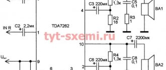
So far, recommendations for improving this scheme:
- The capacity of the input capacitor is 0.56...0.68 µF, and for the subwoofer 1 µF (this is if this capacitor is not used as a subsonic filter).
- C2 = 100 µF x 50V (minimum at 35V).
- C5 = 100 µF x 50V.
- In the power circuit, instead of 100nF capacitors, it is better to use capacitors with a capacity of at least 1 µF 63V. Moreover, non-electrolytic (for example, film K73-17).
- In the power supply circuit it is not necessary to use separate capacitors for each chip. If the microcircuits are installed close, and their power conductors are short and wide, then one capacitor (electrolyte + film) per arm is possible. But we double the capacity of electrolytes.
- Connect a film capacitor with a capacity of at least 0.68 µF in parallel with C5.
- C10 must be designed for a voltage of at least 50V.
- Important! The conductors coming from the outputs of the microcircuits (pins 14), as well as the upper plate of C10, the conductor going to the load, and the conductor going to the resistor R3 (OOS circuit) must be connected at one point. Those. one common point for 5 conductors.
In theory, 3 and 4 microcircuits can be connected in parallel in this way (one master and several assistants), but this is not so good: firstly, there is practically nowhere to raise the supply voltage, and the increase in output power will be negligible. Secondly, it will be more difficult for the “master” to control several “helpers” (which have their own input currents and capacitances), and he may begin to distort the signal.
And don’t forget: in order for an amplifier to supply a large current to the load, this current must first be provided by a source. And if the source is weak... Do not skimp on power filter capacitors.
This is my least favorite scheme. If previous inclusions were provided by the manufacturer, then this one is not. Of course, you can “add” any microcircuit this way, including the TDA7294 / TDA7293, but in my opinion all these add-ons are from the evil one.
Like the “parallel” circuit, this one is designed for low-impedance loads, but in it most of the output current is not removed from the microcircuit, but is supplied to the load by additional bipolar transistors. And the microcircuit only controls them.
This circuit is designed to work with low-impedance loads and is known as the “Chivilch circuit” (Radio No. 11, 2005, taken directly from there, and other circuits are very similar and have the same principle). This particular scheme has many flaws and weaknesses that need to be corrected. A list of corrections of 15 (!) points is attached.
The amplifier on the TDA 7294 is complemented by two powerful output transistors operating in B mode. They enhance the output current of the microcircuit, so less power is dissipated on the microcircuit, which means you can raise the supply voltage to get more power in the load (as well as in “parallel” » diagram).
At rest, the output (that’s what I will now call mounted bipolar transistors - now they are output) transistors are closed and do not consume current from the power source. At a low signal level (up to ~0.5 volts at the load), the transistors do not open, and the output signal flows from the output of the microcircuit to the load through resistor R7 (i.e., the microcircuit puffs alone, and not just like that, but through the resistor) . At the same time, tension appears on it. As the signal level increases, the voltage on R7 increases, and when it reaches ~0.7 volts (this corresponds to a power of 30...50 mW at a 4 Ohm load), the output transistors begin to open. At low output voltages, the output transistors are closed. At low voltages, the transistors open only at loudness peaks for a short time. As the output signal grows (if you turn up the volume), the outputs “increasingly” come into operation, taking over power for the load. At the same time, only 5...15% of the power is supplied from the microcircuit to it (the load) (and another ~10% of the output power is spent by the microcircuit on powering the output transistors). The output transistors operate in class B (and to be honest, in class C, since their cutoff angle is more than 180 degrees, but I won’t scare people). Those. they work in turn: when one of them is open, the other is closed. For example, the upper transistor opens with a positive voltage, and the lower one with a negative voltage. At low output voltage they are both closed. When the additional output transistor is open, the current flows to the load mainly through it. And the microcircuit does not so much power the load as control the operation of this additional transistor.
Thus, you can work on a low-impedance load and get the maximum voltage and current without overheating the microcircuit. Unlike “parallel” connection, here the microcircuit acts as a preliminary stage, and the main power is controlled by additional transistors. And since the transistors operate in class B mode, they do not heat up too much. Everything seems to be covered in chocolate. But there are drawbacks, and considerable ones, if we talk about high sound quality.
Flaws.
- Since the voltage on the microcircuit is limited to 40 Volts, it will not be possible to significantly increase the power supply (and therefore the output power). For a 4 Ohm load this increase will be from approximately 50 W to 80...100 W. If you use the TDA7293, which allows higher supply voltages, you can reach up to 110 W.
- Additional transistors introduce their own nonlinearity, so the overall distortion compared to the microcircuit alone will increase.
- When opening/closing output transistors, additionally (compared to a simple microcircuit) so-called switching distortions are formed - uncontrolled collector current pulses, as well as “step” distortions. And quite large. And since the speed of the microcircuit is low, it does a poor job of suppressing such distortions (using OOS).
- To operate at those moments when the output transistors are closed, and the microcircuit works alone without them, the microcircuit is required to operate at a higher speed (in terms of frequency and rate of rise of the output voltage) than in the normal state.
I will especially explain this last point. Here are oscillograms of the voltage at the load (blue line) and at the output of the microcircuit (red line).
It is clearly visible that the initial sections (close to zero) of the red line are more vertical than the blue one. Here, the output transistors are not yet working, and the microcircuit has to “work faster” in order to power the load not directly, but through resistor R7 (I don’t want to describe the reasons in detail - I’m too lazy to go into theory, that’s a couple of pages more, if it’s detailed). At a voltage of ~0.8 volts, the outputs open, and the output signal of the microcircuit begins to repeat the output signal of the entire amplifier, only 0.8 volts higher.
In fact, this initial section is not so steep - I exaggerated it slightly for clarity. But the microcircuit is also quite slow, and it has to compensate for all these high-frequency “bugs” with the help of OOS. Due to the relatively low frequency of the first pole of the microcircuit, at high frequencies the OOS depth is noticeably reduced, and it is difficult for it to cope with increased distortion. Therefore, the total distortion of the entire amplifier is much greater than that of just a microcircuit.
I once assembled similar systems using high-speed op-amps, supplemented with high-frequency output transistors (i.e., so that everything would work better at high frequencies). As entry-level systems they sounded good. The sound quality (and the level of distortion) here strongly depends on the resistance of resistor R7. The smaller it is, the better. But on the other hand, the lower this resistance, the later (as the signal grows) the overhead outputs open, which means the greater the load on the microcircuit. Those. The more we unload the microcircuit, the more we lose quality. Increasing the quality, we load the microcircuit. The maximum quality will occur at maximum load if the outputs do not turn on at all (that is, if there are no outputs at all!). The results were much better when the outputs were taken out of mode B (a bias voltage was applied to them and a quiescent current appeared). At the same time, the output signal of the microcircuit itself became “more beautiful”, and the sound was better than even with a small resistance R7 in mode B.
If we follow this path: set the output transistors to an initial bias, which will improve the sound, change the control circuit for these transistors to increase the output voltage, change the microcircuit to a high-speed, high-quality op-amp, then we will end up with a completely different amplifier. It will have much better quality and higher power output, but will not contain the TDA7294 chip.
Despite the fact that I personally don’t like this inclusion, there is a use for it, and here I agree with those who do this - in their case, this is really the most optimal solution. One option is a subwoofer operating at a 4-ohm load, and its power is 50...60 W. For just one microcircuit this is already at the limit. A more powerful microcircuit easily provides such power. The second option is the low-frequency/mid-frequency channel of a two-way amplifier (the high-frequency channel is made on a TDA7294 without amplification) - bi-amping - for sounding a room. Again, a power of 50 W is obtained without problems, and working 18 hours a day every day in any weather (even in the summer heat) is easy - the microcircuit is not loaded. And operation at relatively low frequencies is easy for the amplifier. The third option is voice-over of cultural and entertainment events in the open air. There the amplifier can stand in the open air in the sun and work normally. And no one will notice the decrease in sound quality - after all, everyone is having fun (with beer, for example).
So, if anyone still wants to make this circuit, here are some tips:.
| Only bipolar transistors can be used as outputs! For field ones, to open, you need to apply a lot of voltage - about 4 volts, or even more (regardless of whether they are “vertical” or “horizontal”). And this voltage is formed across resistor R7. Its power should be at least 5 W, it will heat up accordingly. And, most importantly, at low power (up to about 5 W) only one microcircuit without outputs will work. And not directly, but through a resistor! And it will be much harder for her... |
- The decrease in quality is least noticeable at low frequencies (the OOS works at full capacity there, and the speed of the microcircuit and transistors is sufficient), so the circuit is suitable for subwoofers.
- Do not exceed supply voltage. 40 volts – maximum (for TDA7293 maximum 44 volts.). There is no point in using low (below 28) - all the advantages disappear: the output power is limited by the power supply and at such a voltage it turns out to be small.
- We increase C2 to 1000 pF (= 1 nF), and for the sub, C2 = 3.3 nF and R1 = 3.3 kOhm.
- C5 = 47...100 µF 50 V. For sub 100 µF. And we connect its “minus” to the output of the microcircuit (to the 14th leg) for the TDA7294, or to the 12th leg for the TDA7293. This will work much better than if you connect a capacitor to the output of the entire amplifier, as in the diagram.
- C9 and C10 at least 1 µF 63 V, for example type K73-17. Even better is 2 of these capacitors in parallel. Moreover, it would be nice to be closer to the transistors.
- The fuses are 5A (and even then they can burn out during volume peaks, especially on the subwoofer, then we set 7.5...10 amp ones).
- Wind coil L 1 directly on resistor R8. To do this, take a resistor of the MLT-2 W type and wind 2 layers of wire with a diameter of 0.7...1 mm around it. The top layer should be shorter so that the coils do not slip. And there is no need to try to fit as many turns there as possible; it is better to do everything carefully. Lightly soak the coil with glue to prevent it from coming apart. We wind the coil terminals onto the resistor terminals and it turns out “two in one”.
- Even though the microcircuit is unloaded, it needs to be cooled. It may be a small radiator, but it should be there. You can put it and the transistors on a common radiator through gaskets.
- After assembling the amplifier, it would be good to make sure that there is no self-excitation or ringing by looking at the signal with an oscilloscope. If these “bugs” are present, then you can try connecting a chain in parallel with resistor R3 consisting of a 100 picofarad capacitor and a 6.8 kOhm resistor connected in series.
- Important! The conductors coming from the emitters of the transistors, as well as the conductors going to resistors R3 (OOS circuit), R7, R8+L1, R9, must be connected at one point. Those. one common point for 6 conductors.
- R5 and R6 are a bit big. Their optimal value: 33…68 kOhm.
- Important! We remove capacitor C3 altogether (so that the 9th leg of the microcircuit is connected to a source without a capacitor - after all, it sets the StdBy mode, therefore, when the mode is on, the output transistors of the microcircuit are disabled, and, therefore, the bases of the external transistors are also disabled!!! this is bad) . If you don’t want to, then the bases of the transistors must be connected to ground through a 10...15 kOhm 0.125 W resistor. But it is necessary to do one of these things - the reliability of the system will increase.
- We take capacitor C4 with a slightly larger capacity: 22...47 µF.
- Important! Capacitors C3 (if any) and C4 are charged to the source voltage (40 volts according to the circuit), so they must have an operating voltage of at least 50V.
- It is better to take resistor R7 more powerful - 0.5 W.
- It would be good to connect a 100...220 uF 25 volt capacitor in series with resistor R4. Otherwise, there may be a noticeable constant at the output.
- And it is better to use output transistors not domestic, but good imported ones, for example MJL21193/MJL21194 or 2SA1943/2SC5200.
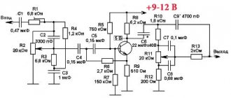
If we are going to do such a thing to increase power, then it would be good to extract this very maximum power (you can extract up to 160 W at a 4 Ohm load). To do this, it is necessary to exclude the influence of supply voltage drops on the microcircuit. Those. stabilize its power supply (precisely the microcircuit - it consumes a small current here, the output transistors are in the span). To do this: We raise the total supply voltage to 50...55 volts (so that even in the most terrible power drawdown there will be 42 volts left) and we power the outputs (since they have the highest current) with an unstabilized voltage - they will withstand. And for the microcircuit we use a +- 38 volt stabilizer, for example, like this one.
The stabilizer is connected to breaks in the power supply circuits of the microcircuit at points A and B. Now power supply voltage drops do not affect the microcircuit, so the power supply to the microcircuit is always maximum and it can always produce the maximum output voltage. This means that the voltage and power at the load will always be the maximum possible. For extreme sports enthusiasts, zener diodes D1 and D4 can be set to a voltage of 15 volts. But the microcircuit will already work at its limit, so I don’t recommend it. But if you use the TDA7293 chip, then it’s easy. The limit here is that all zener diodes are 15 volts + good (without an insulating gasket on the radiator) cooling of the microcircuit. Only now for the outputs a larger radiator is needed. And the stabilizer transistors need to be installed on radiators. I told you - it’s better to immediately make an amplifier that will handle everything... For example, like this.
19.03.2007
Total Page Visits: 5838 — Today Page Visits: 3
More voltage → more power
There are two important benefits associated with a bridge amplifier. The first thing we'll discuss is this: a bridge amplifier allows you to significantly increase the power delivered to your load. How much more? Well, we know that the instantaneous power of an AC voltage signal can be expressed as follows:
\[P_{load} = \left( \frac{V_{peak}}{\sqrt{2}} \right)^2 \times \frac{1}{R}\]
Thus, the power is proportional to the square of the peak voltage. The bridge circuit doubles the voltage across the load; therefore, it provides a fourfold increase in the power delivered to the load. You might be wondering - why can't we just use one op amp and increase the gain to get more voltage? Why bother with a bridge circuit? These are good questions, and the answer is that a bridge amplifier produces Pload that is four times the maximum power you can achieve at a given supply voltage. In other words, a bridge amplifier is especially useful when you are trying to get as much power as possible from your power rail.
In this age of low voltage systems, you may find that the supply voltage is the limiting factor in how much power you can supply to the load. Let's assume that the load resistance is fixed, so you can't increase power by decreasing Rload, and let's also assume that you have sufficient current available from your power supply. In this case, your 3.3V power supply is holding you back - you could easily supply more power if you had a slightly higher supply voltage. Well, that's where a bridge amplifier comes in: the same voltage rail, but four times the power.
Circuit design of a single-board 4-channel class AB amplifier on a TDA7850 chip
Let's look at the amplifier board vertically from above and figure out what's what here:
This ULF board has its own name, indicated in the lower left corner: HW-452.
There are a lot of elements on the board, even though the “main” TDA7850 chip requires almost no wiring. This is due to the location on the board of two BA3121F noise suppression chips with their own wiring.
Noise suppression microcircuits (each for two channels) work in a very simple way: they subtract the interference signal coming through the ground wire from the signal source from the voltage on the signal wires themselves, which is the sum of “signal + noise”.
As for the wiring of the TDA7850 amplifier chip, it consists of only four rectangular blue capacitors that “cut off” the DC component from the input. You also need several blocking capacitors for power supply and some control elements for the “MUTE” (short-term mute) and “ST-BY” (low-power sleep mode) signals, if there is a need to use them (on this board there are contacts for connecting buttons control of these signals is not provided).
The diagram for using the microcircuit from the datasheet for the TDA7850 microcircuit is as follows (block diagram and example of a circuit diagram):
The microcircuit is equipped with various types of protection: from overheating, from short circuit to ground or to power, from overcurrent, etc.
Note: the numbering of elements on the diagram does not match the numbering on the board.
Now let's go over the other elements of the board.
The two-pin terminal block at the bottom left is the power supply, next to it is the power filtering choke.
Additional filtering is provided by a powerful 10,000 uF 25 V electrolytic capacitor almost in the center of the board. We consider such a high capacity to be an unconditional “advantage” of the board.
Under the inductor there is an LED indicating that power is supplied to the board.
The two black connectors are designed to connect signals through two round 3-pin male 3.5 mm jack connectors.
Two white connectors are connected to them in parallel for connecting the signal using rectangular connectors.
There are two 4-pin terminal blocks on the sides, each with two bridge outputs.
We won’t consider the rest of the “small things” on the board.
No coupling capacitor required
My favorite feature of a bridge amplifier is that it allows you to eliminate DC offset voltage without eliminating DC offset voltage... or something like that. Let's say you have a speaker that you need to connect to your circuit with a single-supply power supply. All audio signals have a DC offset that keeps the negative portions of the sine wave above ground. But the signal we send to the speaker must be pure AC voltage; DC offset voltage in an audio signal reduces dynamic range and promotes distortion. This problem is often solved by using a DC blocking capacitor (also called a coupling capacitor), but this approach has disadvantages: first, the capacitor can be large enough (often hundreds of microfarads) to avoid attenuation of low-frequency components of the signal; Secondly, you need to worry about transient effects associated with the charging or discharging of the coupling capacitor, such as artifacts such as "clicks" and "pops" that interfere with audio reproduction.
Fortunately, if you have a bridge amplifier, there is no need for an isolation capacitor. An additional feature of inverted and non-inverted signals is that the DC offset voltage of one signal can cancel the DC offset voltage of the other:
Figure 5 – Offset voltage compensation
Bridge circuit for 4 LM3886
And this is much more complicated, but the power is almost 2 times higher, about 200 watts. Great for high quality subwoofer. In any case, before you start assembling the amplifier, study this documentation for the microcircuit, which details the nuances of bridging the LM3886.