Have a good time everyone. Let me introduce a power inverter for powering a powerful audio amplifier. Unfortunately, there are few such projects on the Internet, especially well-replicated ones. Therefore, it was decided to make such a power source from scratch. It took a lot of time to design, build and test this UPS. And now, having carried out the last tests (all tests were successful), we can say that the project is completed and it can be presented to the respected amateur radio audience of the site 2 Schemy.ru
The project of this inverter is excellent for UMZCH on 2x TDA7294, in fact, it was developed for it. The converter is not complicated and should be successfully assembled by not very advanced electronics engineers. You don't even need an oscilloscope to run it, but of course it would be useful. The basis of the power supply circuit is m/s TL494.
It is short circuit protected and should provide 250W of continuous power. The converter also has an additional output voltage of +/- 9..12 V, which will be used to power the preamplifier, fans, etc.
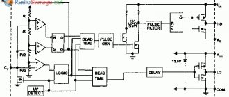
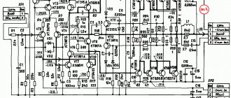
↑ Switching power supply diagram
The scheme is quite simple:
It is a half-bridge inverter with a switching saturable transformer. Capacitors C1 and C2 form a voltage divider for one half of the half-bridge, and also smooth out the ripples of the mains voltage. The second half of the half-bridge is transistors VT1 and VT2, controlled by switching transformer T2. The diagonal of the bridge includes the primary winding of the power transformer T1, which is designed so that it does not become saturated during operation.
To reliably start the converter, a relaxation generator is used on a VT3 transistor operating in avalanche mode. Briefly the principle of its operation. Capacitor C7 is charged through resistor R3, while the voltage at the collector of transistor VT3 increases in a sawtooth manner. When this voltage reaches approximately 50 - 70V, the transistor opens like an avalanche, and the capacitor is discharged through transistor VT3 to the base of transistor VT2 and winding III of transformer T2, thereby starting the converter.
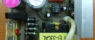
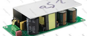
↑ Printed circuit board
The parts of the device, except for the power transformer T1 and powerful transistors VT1, VT2, are mounted on a printed circuit board measuring 150x70 mm (see Fig. 2), made of foil fiberglass laminate.
Rice. 2. Placement of parts on the printed circuit board. The tracks are shown “in the light”, smd elements C9, C10, C23, C24, R9, R10 are installed on the side of the printed tracks
It is advisable to additionally solder the “power” tracks on the printed circuit board on top with tinned mounting wire with a diameter of 0.5 - 0.7 mm.
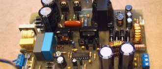
↑ Design and details of the UPS
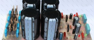
The power supply is assembled on a printed circuit board made of single-sided fiberglass. I don’t provide a drawing of the board, since everyone has their own parts in their stash. I’ll limit myself to just a photo of my board:
In my opinion, there is no point in ironing such a board, it is too simple.
As transistors VT1 and VT2, you can use domestic KT812, KT704, KT838, KT839, KT840, that is, with a collector-emitter boundary voltage of at least 300V; of the imported ones, I know only J13007 and J13009, they are used in computer power supplies. The diodes can be replaced with any other powerful pulsed ones or with a Schottky barrier; for example, I used imported FR302.
Transformer T1
wound on two folded rings K32×19X7 made of ferrite grade M2000NM, the primary winding is wound evenly throughout the entire ring and is 82 turns of PEV-1 0.56 wire. Before winding, it is necessary to round off the sharp edges of the rings with a diamond file or fine sandpaper and wrap them with a layer of fluoroplastic tape, 0.2 mm thick, and also wrap the primary winding. Winding III is wound with PEV-1 0.56 wire folded in half and is 16+16 turns with a tap from the middle. Winding II is wound with two turns of MGTF 0.05 wire, and is located in a place free from winding III.
Transformer T2
wound on a ring K10×6X5 made of ferrite of the same brand. All windings are wound with MGTF 0.05 wire. Winding I consists of ten turns, and windings II and III are wound simultaneously in two wires and make up six turns.
Stabilizer or filter?
Surprisingly, most often simple circuits with a transformer, rectifier and smoothing capacitor are used to power power amplifiers. Although most electronic devices today use stabilized power supplies. The reason for this is that it is cheaper and easier to design an amplifier that has a high power supply ripple suppression coefficient than to make a relatively powerful stabilizer. Today, the ripple suppression level of a typical amplifier is about 60 dB for a frequency of 100Hz, which practically corresponds to the parameters of a voltage stabilizer. The use of direct current sources, differential stages, separate filters in the power supply circuits of the stages and other circuit techniques in amplifier stages makes it possible to achieve even greater values.
The power supply to the output stages is most often made unstabilized. Due to the presence of 100% negative feedback, unity gain, and the presence of OOOS, the penetration of background and supply voltage ripples into the output is prevented.
The amplifier's output stage is essentially a voltage (supply) regulator until it enters clipping (limiting) mode. Then the supply voltage ripple (100 Hz) modulates the output signal, which sounds simply terrible:
If for amplifiers with unipolar power supply only the upper half-wave of the signal is modulated, then for amplifiers with bipolar power supply both half-waves of the signal are modulated. Most amplifiers are characterized by this effect at high signals (powers), but it is not reflected in any way in the technical characteristics. In a well designed amplifier, clipping should not occur.
To test your amplifier (more precisely, the power supply of your amplifier), you can conduct an experiment. Apply a signal to the amplifier input with a frequency slightly higher than you can hear. In my case, 15 kHz is enough :(. Increase the amplitude of the input signal until the amplifier goes into clipping. In this case, you will hear a hum (100 Hz) in the speakers. By its level you can evaluate the quality of the amplifier's power supply.
Warning! Be sure to turn off the tweeter of your speaker system before this experiment, otherwise it may fail.
A stabilized power supply avoids this effect and leads to reduced distortion during prolonged overloads. However, taking into account the instability of the network voltage, the power loss on the stabilizer itself is approximately 20%.
Another way to reduce the clipping effect is to feed the stages through separate RC filters, which also reduces the power somewhat.
This is rarely used in serial technology, since in addition to reducing power, the cost of the product also increases. In addition, the use of a stabilizer in class AB amplifiers can lead to excitation of the amplifier due to the resonance of the feedback loops of the amplifier and stabilizer.
Power losses can be significantly reduced if you use modern switching power supplies. However, other problems arise here: low reliability (the number of elements in such a power supply is significantly larger), high cost (for single and small-scale production), high level of RF interference.
A typical power supply circuit for an amplifier with an output power of 50W is shown in the figure:
The output voltage due to smoothing capacitors is approximately 1.4 times greater than the output voltage of the transformer.
↑ Setting up the UPS
ATTENTION!!!
THE PRIMARY CIRCUIT OF THE PSU IS UNDER MAINS VOLTAGE, SO PRECAUTIONS SHOULD BE FOLLOWED WHEN SETTING UP AND OPERATING. It is advisable to start the unit for the first time by connecting it through a current-limiting resistor, which is an incandescent lamp with a power of 200 W and a voltage of 220 V. As a rule, a properly assembled power supply does not need adjustment, the only exception is the VT3 transistor. You can check the relaxer by connecting the emitter of the transistor to the negative pole. After turning on the unit, sawtooth pulses with a frequency of about 5 Hz should be observed on the transistor collector.
Resistors
The resistors are all either Soviet MLT or foreign, quite low-watt. The exception is resistors R16 and R17, with a nominal value of 10 kOhm and a power of 10 W; they are made from high-resistance wire, which is wound onto a frame.
On the diagram
| Options | Qty | Replacement | Purchase | |
| Resistors | ||||
| R1 | 180k 1 W | 1 | ————- | 180k 1 W |
| R2 | 1k 0.25 W | 1 | ————- | 1k 0.25 W |
| R3 | 8.2k 0.125 W | 1 | ————- | 8.2k 0.125 W |
| R4-R5 | 6.8k 0.125 W | 2 | ————- | 6.8k 0.125 W |
| R6-R7 | 1.6k 0.125 W | 2 | ————- | 1.6k 0.125 W |
| R8-R9 | 270 Ohm 0.25 W | 2 | ————- | 270 Ohm 0.25 W |
| R10-R11 | 390 Ohm 0.25 W | 2 | ————- | 390 Ohm 0.25 W |
| R12-R13 | 51 Ohm 0.125 W | 2 | ————- | 51 Ohm 0.125 W |
| R14-R15 | 2k 0.125 W | 2 | ————- | 2k 0.125 W |
| R16-R17 | 10k 10W | 2 | ————- | 10k 10W |
Diodes
| On the diagram | Options | Qty | Replacement | Purchase |
| Diodes | ||||
| VD1-VD4 | D246 | 4 | 1N2025, BZX29C35V6, 40112, 1N1063, 1N1069, 1N1092, 1N1092A, 1N1614A, 1N1623(24), 1N2025, 1N2234, 1N2235, 1N2254, KD202K, KD202M , KD202R, KD206B, D247B | bridge 10A, 1000V |
| VD5 | KTs402D | 1 | —————— | bridge 1A, 1000V |
| VD6 | D810 | 1 | 1SS174, ZR937-50, ZR936-50, D814V | D814V |
| VD7-VD12, VD21 | KD212A | 7 | 1N1124, 1N3361 | KD212A |
| VD13-VD20 | KD2997A | 8 | 1N248, 1S421, 1N248, 1S421, KD2997B, KD2999B | KD2997A |
Field effect transistors
Transistors can operate in amplification mode and switching mode. It is preferable to use field-effect transistors in switching mode. The field effect transistor is voltage controlled. If a constant voltage is applied to the source (the place from which the current will flow) and the drain (where the current will flow), and a high-frequency voltage is applied to the control electrode (gate), then with the frequency of the voltage applied to the gate, current will flow between the source and drain. This is the principle of the key circuit. If you use two keys, each opened by a gate at its own non-overlapping time, and apply the voltage removed from the drains to a pulse transformer, then an alternating high-frequency voltage can be removed from the output of this transformer.
You can take any field-effect transistors, but they must be installed on radiators. If the power of the unit is 800 W, then the transistor does not necessarily have to dissipate 800 W. In switching mode, the transistor hardly heats up, but it is better that the power dissipation of each transistor is about 100 W. The parameters by which field-effect transistors should be selected are: firstly, the gate-source voltage (>14 V), and secondly, the drain-source voltage (>750 V). When using two transistors and a transformer with a midpoint, the voltage at the drain - source of each field switch will be equal to 2.4 * U, i.e. 2.4 * 310 = 744 V. If you set the field switches to Uc = 600 V, it breaks them very beautifully with a loud bang and the entire crystal flying into the air. According to the circuit, you need to use KP707V2 transistors.
Rectifier
After the transformer, the voltage is rectified on a high-frequency bridge. Diodes are quite powerful, so they need radiators. Radiators can be made from a duralumin profile so that the pressure plate on top completely covers the diode body. One of the diode leads, usually the anode, is connected to a tinned copper case, so you need at least 3 radiators, and preferably 4. Moreover, if you make 2 diode bridges, then the number of radiators doubles, increasing the volume of the block.
Transistors
| On the diagram | Options | Qty | Replacement | Purchase |
| Transistors | ||||
| VT1 | KT817B | 1 | BD175, KT817, KT819 | KT819G |
| VT2 | KT315G | 1 | KT315, KT503, KT3102 | KT503E |
| VT3-VT4 | KT315B | 2 | KT315, KT503, KT3102 | KT503E |
| VT5-VT6 | KT361E | 2 | KT361, KT502, KT3107 | KT502D |
| VT7-VT8 | KT3102ZH | 2 | BC183A, BC546B, BC547B | BC548 |
| VT9-VT10 | KP707V2 | 2 | IRFBE32, 2SK1117, KP707V1, KP707E1 | P6NK90ZFP |
Microcircuits
The board is designed so that all the parts are on one side, and the microcircuits are on the other, i.e. from the side of the tracks. Between pins 7 and 14 of each microcircuit, i.e. You can solder 0.01 µF paper capacitors between the power legs - this will improve the situation with ripple.
| On the diagram | Options | Qty | Replacement | Purchase |
| Microcircuits | ||||
| DA1 | K561LA7 | 1 | K176LA7, K564LA7 | K561LA7 |
| DA2 | K561TM2 | 1 | K176TM2, K565TM2 | K561TM2 |
| DA3 | K561LA8 | 1 | K176LA8, K566LA8 | K561LA8 |