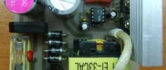
Nowadays ready-made modules of pulse voltage converters based on the LM2596 chip have become available.
Quite high parameters are declared, and the cost of the finished module is less than the cost of the parts included in it. The small size of the board is attractive. I decided to purchase a few and test them out. I hope my experience will be useful to less experienced radio amateurs.
↑ It’s hard to call it a stabilizer...
You might think that it is enough to take a transformer, a diode bridge, connect a module to them, and we have a stabilizer with an output voltage of 3...30 V and a current of up to 2 A (short-term up to 3 A).
That's exactly what I did. Without load everything was fine. A transformer with two windings of 18 V and a promised current of up to 1.5 A (the wire was clearly too thin by eye, and so it turned out). I needed a +-18 V stabilizer and I set the required voltage.
With a 12 Ohm load the current is 1.5 A, here is the waveform, 5 V/cell vertical.
It can hardly be called a stabilizer.
The reason is simple and clear: the capacitor on the board is 200 uF, it serves only for the normal operation of the DC-DC converter. When voltage was applied to the input from a laboratory power supply, everything was fine. The solution is obvious: you need to power the stabilizer from a source with low ripples, i.e. add a capacitance after the bridge.
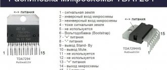
Stabilized power supply for UMZCH
Stabilized bipolar power supply ±36 V for class AB UMZCH. The report is 20 years late. Designed for a prepared reader. 1.
The original circuit was published in the magazine “Radio” (1987, No. 8, p. 31) “UMZCH supply voltage stabilizer”:
In 2000, when assembling another amplifier, this circuit was recommended to me by an employee with the words “it should work.” As a bonus, I was presented with transistors KT825 and KT827 (several pieces of each).
Highlights of the scheme:
- powerful transistors “sit” on radiators without insulating gaskets - ballast resistors R4 and R5 are connected crosswise to the outputs of the stabilizers, i.e. a higher stabilization coefficient is obtained - when turned on, the stabilizer “does not pick up” if there is a short circuit in some arm. or load resistance is less than a certain value
2.
Known implementations of this scheme. There are few of them (on the Internet; in reality, of course, there are more). Here is one of them:
According to the author, the circuit “starts unstably at a high load current, and the current when the output is closed is not standardized and depends on the transfer coefficients of the transistors used, which sometimes leads to their failure. Over the past time, new electronic components have appeared, powerful field-effect transistors have become available, which prompted the author to experiment with a computer model of the device proposed by V. Oreshkin, which was created in the LTspice IV simulator, and improve it. The power supply circuit born as a result of such experiments is shown in Fig. 2." ©
Whether this scheme was tested live or only in a simulator is not known for certain.
3.
TK for BP.
The UMZCH load then was the modified S-90 (4 Ohms). About the modification of the S-90.
Analysis of other people's circuits led to disappointing conclusions: all f... people have learned to hold a soldering iron, but they do not understand what they are doing. In total, three pairs of S-90 speakers were modified. The circuit is our own, calculated in the EWB512 simulator; has never been made publicly available anywhere. The last pair of speakers was tested in wiretapping on the appropriate equipment, which confirmed the correctness of the calculations.
I wanted to have 2*100W at 4 Ohms for each channel. Load voltage (RMS) U = sqrt(100*4) = 20 (V) Load current (RMS) I = 20 /4 = 5 (A) Load current (peak) = 5*1.41 = 7.1 ( A)
Since the emphasis was on power and reliability, the following characteristics (aka TZ) were conceived: - supply voltage ±36 V - load current 2.5A (long-term for each polarity) - load current 25A (short-term for each polarity)
4.
The power supply was assembled (or built, which is the correct way to say it) from scrap materials and used radio components. Transformers - Polish UNITRA B-4247-147-4
According to fragmentary information from the Internet, the power of the transformer is 80W. The main secondary winding is 2*17V with a tap from the middle, plus a couple of additional windings “on the tails” of 1V each. Those. you can use either 2*17V 2.5A or 2*18V 2.5A.
The low-current secondary has not been tested.
Diode bridges - four D232 diodes on radiators.
Capacitors: KEA -II 66000uF*63V after each bridge (2*33000uF).
The original circuit did not want to start normally on the KT825-KT827 transistors: the first time it was turned on, the KT827 (which is npn) broke through. Why exactly the 827 was not important, but the stock of donated KT827s quickly dried up, and there was a non-working circuit on the table with which something had to be done.
The choice of powerful transistors was meager: 2N3055 in unlimited quantities and KT837V, which were used in manufactured devices (at work). I had to abandon the component KT825-827 and assemble a circuit “from what I had” ©.
To provide a peak current of 30A, we had to parallel the transistors: - 4*KT837V (i.e. 4*7.5=30A) - 3*2N3055 (i.e. 3*10=30A) Naturally, with the corresponding emitter resistors.
The final scheme (the simulator is used only as a drawing tool):
By the way, the circuit does NOT work in the simulator. )))
List of elements: - transformer UNITRA B-4247-147-4 - 2 pcs. — rectifier diodes D232 — 8 pcs. — capacitors KEA-II 33000 uF * 63V — 4 pcs. — capacitors C5, C6 — 2000 uF * 63V — 2 pcs. — zener diodes VD1, VD3 — D815G — 2 pcs. VD2, VD4 - D816B - 2 pcs. — transistors VT1 — 3 pcs. in parallel 2N3055 with emitter resistors 0.1 Ohm (can be increased to 0.2 Ohm) VT2 - 4 pcs in parallel KT837V with emitter resistors 0.13 Ohm (can be increased to 0.27 Ohm) VT3 - 2SA1837 (KT816 was originally installed ; replacement of VT3, VT4 - in 2005, the rest - unchanged) VT4 - 2SC4793 (KT817 was originally installed) R1, R2 - PEV-7.5 270 Ohm - 2 pcs. R5, R6 - MLT-2 2.2 kOhm - 2 pcs.
Circuit protection (not shown in the diagram): - a pair of 5 A fuses (one for each polarity) - 3 A (before the primary winding)
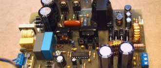
PSU assembly:
Dimensions: 440*362*80 mm. Weight 8.5 kg.
The top cover is held in place by 18 M3 screws. He unscrewed it and took off the cover. PSU inside:
An electronics engineer friend, looking at all this, said: “Either the transformers are small, or the capacitors are large.” ))
2N3055 on the right radiator:
KT837V on the left radiator:
5.
Measurements. Working with a 14 Ohm resistive load (2.5A from each polarity) is of no interest: everything works. I was interested in the reaction of the power supply to a significant increase in current consumption.
Experiment conditions: - power supply load - 2*100W UMZCH with 4 Ohm resistors connected to the output of each channel - test signal - 200 ms 40 Hz tone sending from a software generator (SpectraLab) to the input of each UMZCH channel
Oscillogram of the output of one of the channels (divider 1:10)
±24 V amplitude, it was not possible to turn it up more, because all mixer engines are already at maximum.
Next, I used the two-channel metering mode. “Closed” input of the 2nd channel for the +36 V power line (divider of the 2nd channel 1:1):
“Closed” input of the 2nd channel for the minus 36 V power line (2nd channel divider 1:1):
The drawdown along the power lines is about 0.5 V (the noise that the oscilloscope picked up does not count; it has such a drawback).
We consider: delta I = (24V/4Ohm) * 2 = 12 (A)
PSU output impedance: Rout. = delta Uout. / delta I = 0.5V / 12A = 0.042 (Ohm)
IMHO, very good.
6. Conclusions:
— technical specifications completed — reliability tested by time (20 years, normal flight) — assembly costs — only personal time and a minimum of parts
Instead of a cat
Happy amplifier launches to everyone!
PS
Please, do not post a button accordion in the form of a picture “I didn’t understand anything, but it’s very interesting.”
Additional Information
Video blogger Sergei Demekhov, who is in the photo, is no longer with us.
↑ Fighting ripples
Here is the voltage with a load of 1.5 A at the input of the module without an additional capacitor.
↑ Increased input capacitance
With an additional 4700 uF capacitor at the input, the output ripple decreased sharply, but at 1.5 A it was still noticeable. When reducing the output voltage to 16V, the ideal straight line (2V/cell).
The voltage drop across the DC-DC module should be at least 2...2.5 V.
Now you can watch the ripple at the output of the pulse converter.
Small pulsations with a frequency of 100 Hz modulated with a frequency of several tens of kHz are visible.
↑ LC filter at output
The Datasheet on the LM2596 recommends an additional LC filter on the output. That's what we'll do. As a core, I used a cylindrical core from a faulty computer power supply and wound the winding in two layers with 0.8 mm wire.
The board shows in red the place for installing a jumper - the common wire of two channels; the arrow shows the place for soldering the common wire, if you do not use terminals.
Let's see what happened to the HF pulsations.
They are no longer there. Small pulsations with a frequency of 100 Hz remained. Not perfect, but not bad.
I note that as the output voltage increases, the inductor in the module begins to rattle and RF interference at the output sharply increases; as soon as the voltage is slightly reduced (all this with a load of 12 Ohms), the interference and noise completely disappear.
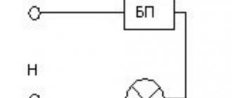
Speaker return current
As you know, the acoustic system is a reactive load. This means that it can return current to the amplifier. This current, flowing through the conductors, creates a potential difference, which can lead to positive feedback and, as a result, instability of the amplifier.
To avoid this, the speaker ground terminal should be connected to the common terminal of the power filter capacitors. Often the speaker terminal is connected to the common terminal of the microcircuit, as shown in the figure:
This connection closes the negative half-wave of the signal into a local loop, eliminating the filter capacitor that could reduce radiated interference and improve system stability.
The figure shows how the ground leakage current of one half-wave of the signal can cause unpleasant noise and distortion if the common wire of the speaker is connected to the output stage of the microcircuit:
Similarly, if on the amplifier board in the power circuits there are bypass capacitors (and they usually are) of a fairly large capacity of several hundred microfarads, then the charging current pulses will also create a potential difference on the common conductor. Therefore, we repeat once again, the best point for connecting the common wire of the speaker system is the common terminal of the power filter capacitors.
↑ Final diagram for connecting LM2596 modules
The scheme is simple and obvious.
With a long-term load of 1 A current, the parts heat up noticeably: the diode bridge, the microcircuit, the module choke, most of all the choke (additional chokes are cold).
Heating to the touch is 50 degrees. When operating from a laboratory power supply, heating at currents of 1.5 and 2 A is tolerable for several minutes. For long-term operation with high currents, a heat sink to a larger chip and inductor is desirable.
Mono amplifier installation example
Typically, the star in a single-supply amplifier is three-pointed: the signal ground, the power filter capacitor ground, and the dirty ground. An example is shown in the figure:
click to zoom
Here, an amplifier should be understood as both an integrated design and amplifiers based on discrete elements.
As you can see, the signal ground is connected to one beam - the currents here are very small, so there is no need to connect all elements with separate conductors. to the second beam by separate conductors : the output stage, the Zobel circuit, the common terminal of the speaker system and bypass capacitors. The common terminal of the filter capacitor of the power supply is connected to the third beam.
The correct connection of the common wire to the pins of the microcircuits is shown in the figure:
Option "c" is an incorrect option. Due to the resistance of the track, a large current will raise the potential of the low-current common wire relative to the output of the microcircuit, which will lead to an increase in distortion.
To be continued…
The article was prepared based on materials from the magazine “Practical Electronics Every Day”
Author: Jack Roseman
Free translation: Editor-in-Chief of RadioGazeta
↑ Installation
To mount the module, I used homemade “stands” made of tinned wire with a diameter of 1 mm.
This ensured convenient installation and cooling of the modules.
The posts can get very hot when soldering and will not move like simple pins. The same design is convenient if you need to solder external wires to the board - good rigidity and contact. The board makes it easy to replace the DC-DC module if necessary. General view of the board with chokes from halves of some kind of ferrite core (inductance is not critical).
Despite the tiny dimensions of the DC-DC module, the overall dimensions of the board turned out to be comparable to an analog stabilizer board.
Circuit design
The case was used from a non-working computer power supply. The switch and connector for the power cord remained in their original place. I have this transformer. I couldn’t find any information about it on the Internet, so I looked for the primary and secondary windings myself.
Let me remind you: when dialing an unknown transformer, you need to connect it to the network through a light bulb!
In my case, it turned out that it has 4 windings of 10 volts. I connected the windings in series - it turned out 2 x 20 volts or 1 x 40 volts. I have two diode bridges: one for +/-28 volts and the second +/-14, I made it to test circuits on operating systems (low-pass filters, tone blocks, and others).
To test the zener diodes, the simplest well-working circuit was chosen, which is on another site. I only changed the values of resistors R1 and R2: R1 - 15k, R2 - 10k. And accordingly, it is powered by me from 56 volts. Placed it on a small piece of PCB. I made the scarf by cutting tracks. I took the Soviet button, since it is easier to attach to the front panel. The contacts for connecting zener diodes were placed on the front panel. I did not place the voltmeter on the panel; I removed 2 terminals for connecting a multimeter. I also placed the diode bridges with capacitors on pieces of PCB: of course, they could have been placed on one board, there were just a few “offcuts”, so I placed them on them. Power outputs for connecting the devices under test were implemented on wiring terminals. In general, this is the schematic.
↑ Conclusions
1. A transformer with a high-current secondary winding or with a voltage reserve is required; in this case, the load current may exceed the current of the transformer winding.
2. At currents of the order of 2 A or more, a small heat sink to the diode bridge and the 2596 microcircuit is desirable.
3. It is desirable to have a large capacity power capacitor, this has a beneficial effect on the operation of the stabilizer. Even a large and high-quality container heats up a little, therefore a low ESR is desirable.
4. To suppress ripple with the conversion frequency, an LC filter at the output is required.
5. This stabilizer has a clear advantage over a conventional compensation one in that it can operate in a wide range of output voltages; at low voltages, it is possible to obtain an output current greater than what the transformer can provide.
6. The modules allow you to make a power supply with good parameters simply and quickly, bypassing the pitfalls of making boards for pulse devices, that is, they are good for beginner radio amateurs.
Denouement
When using two filter capacitors with bipolar power supply, you must ensure that the two half-waves of the signal are summed at one point , as shown in the figure:
Often, using a single capacitor connected between the plus and minus of the power supply can solve this problem. This method works well with 5532 op amps and LM3886 power amplifiers.
When the driver stage and output stage are powered separately, this can cause some instability in the amplifier at high frequencies. The problem is solved by connecting a small-capacity ceramic capacitor between the power pins of the microcircuit:
click to zoom
If the capacity of the bypass (blocking) capacitors is more than 100 µF, their common wire should be connected to the “dirty” ground, since large charging currents can create noticeable interference if the capacitors are connected to the signal ground.