Based on the IR2153 chip and power IGBT transistors, many circuits have been designed, such as an induction heater driver and generator, a Tesla coil power supply, DC-DC converters, switching power supplies, and so on. And the combination NGTB40N120FL2WG + IR2153 work together perfectly, where IR2153 is the driver - the master pulse generator, and a pair of bipolar transistors with an insulated gate of 40A/1000V can handle a large load current.
IR2153 connection diagrams
Schematic diagram of IR2153 connection
IR2153 – power supply electrical circuit
Tesla circuit on IR2153
If you are going to repeat one of these circuits, here is an archive with printed circuit board files. The gate pulse generator circuit for controlling them operates from 15 V DC - up to 400 V voltage is supplied to the transistors of the output stage.
IR2153 switching power supply on board
By the way, the IR2153 is an improved version of the popular IR2155 and IR2151 ICs, which includes a high-voltage half-bridge gate driver. The IR2153 provides more features and is easier to use than previous m/s. There is a shutdown feature so that both gate driver outputs can be turned off using a low signal voltage. Noise immunity has been significantly improved, both by reducing peak pulses. Finally, special attention has been paid to providing as comprehensive ESD protection as possible on all terminals.
Four switching power supplies on IR2153
I would like to present to your attention four different circuits of switching power supplies based on everyone’s favorite popular IR2153. All these schemes were collected and tested by me in 2013-2015. Now, in 2022, I dug up all these schemes in my archives and am in a hurry to share with you. Don’t be confused by the fact that not all diagrams have photos of assembled devices, and that the photos will also include incompletely assembled power supplies, but that’s all I was able to find in my archives.
So the first power supply, let’s call it “high-voltage”:
The circuit is classic for my switching power supplies. The driver is powered directly from the network through a resistor, which reduces the power dissipated by this resistor compared to power supply from the +310V bus. This power supply has a soft start (inrush current limiting) circuit on the relay. Soft start is powered through quenching capacitor C2 from a 230V network. This power supply is equipped with protection against short circuit and overload in secondary circuits. The current sensor in it is resistor R11, and the current at which the protection is triggered is regulated by trimming resistor R10. When the protection is triggered, the HL1 LED lights up. This power supply can provide a bipolar output voltage of up to +/-70V (with these diodes in the secondary circuit of the power supply). The pulse transformer of the power supply has one primary winding of 50 turns and four identical secondary windings of 23 turns each. The wire cross-section and transformer core are selected based on the required power that must be obtained from a particular power supply.
The second power supply, we will conventionally call it a “self-powered UPS”:
This unit has a circuit similar to the previous power supply, but the fundamental difference from the previous power supply is that in this circuit, the driver powers itself from a separate winding of the transformer through a quenching resistor. The remaining nodes of the circuit are identical to the previous presented circuit. The output power and output voltage of this unit is limited not only by the parameters of the transformer and the capabilities of the IR2153 driver, but also by the capabilities of the diodes used in the secondary circuit of the power supply. In my case it is KD213A. With these diodes, the output voltage cannot be more than 90V, and the output current cannot be more than 2-3A. The output current can be higher only if radiators are used to cool the KD213A diodes. It is worth additionally stopping at the T2 throttle. This inductor is wound on a common ring core (other types of cores can also be used), with a wire of a cross-section corresponding to the output current. The transformer, as in the previous case, is calculated for the appropriate power using specialized computer programs.
Power supply number three, let’s call it “powerful with 460 transistors” or simply “powerful 460”:
This scheme is already more significantly different from the previous schemes presented above. There are two main big differences: protection against short circuit and overload here is made on a current transformer, the second difference is the presence of two additional transistors in front of the keys, which allow isolating the high input capacitance of powerful switches (IRFP460) from the driver output. Another small and insignificant difference is that the limiting resistor of the soft start circuit is located not in the +310V bus, as was the case in previous circuits, but in the 230V primary circuit. The circuit also contains a snubber connected in parallel with the primary winding of the pulse transformer to improve the quality of the power supply. As in previous schemes, the sensitivity of the protection is regulated by a trimming resistor (in this case R12), and the activation of the protection is signaled by the HL1 LED. The current transformer is wound on any small core that you have at hand, the secondary windings are wound with a wire of small diameter 0.2-0.3 mm, two windings of 50 turns each, and the primary winding is one turn of wire of a cross-section sufficient for your output power.
And the last pulse generator for today is a “switching power supply for light bulbs,” let’s call it that.
Yes yes, don't be surprised. One day there was a need to assemble a guitar preamplifier, but I didn’t have the necessary transformer at hand, and then this impulse generator, which was built just for that occasion, really helped me out. The scheme differs from the previous three in its maximum simplicity. The circuit does not have protection against short circuits in the load as such, but there is no need for such protection in this case, since the output current on the secondary +260V bus is limited by resistor R6, and the output current on the secondary +5V bus is limited by the internal overload protection circuit of the stabilizer 7805. R1 limits the maximum starting current and helps cut off network noise.
General recommendations:
- The pulse transformer for each circuit must be calculated in accordance with your personal requirements for the power supply and your capabilities, so I do not provide specific winding data.
- To calculate a pulse transformer, it is very convenient to use the “Old Man” programs - Lite-CalcIT and RingFerriteExtraSoft.
- Before connecting the switching power supply to the network, you must carefully check the installation for errors, “snot” on the board, etc.
- It is imperative to wash the board on the installation side with gasoline, acetone, kerosene, any solvent or alcohol to completely remove flux residues. A switching power supply operates at a high frequency and even a slight parasitic conductivity or capacitance can lead to the fact that the power supply assembled from serviceable parts will not work or will explode the first time it is turned on.
- The first switching on must be done only with a current limitation; it can be limited either by a powerful resistor or a powerful incandescent lamp, there may be other options.
- It is necessary to remember and never forget about electrical safety rules. Each of the power supply circuits contains life-threatening voltage.
Attention! When buying an IRF740, you need to be extremely careful not to run into a fake, which is very common, especially on Aliexpress, for this it is important to know what a fake IRF740 looks like.
The illustration above shows two types of original IRF740 made by Vishay and made by IR, as well as a typical fake that is often found on Aliexpress and other stores.
In addition to appearance, a fake can be easily distinguished from an original using a transistor tester:
If you install an original transistor in the transistor tester socket, the displayed capacitance value will be: C=2.6…2.7 nF. Counterfeits have a much smaller crystal than the original transistor and therefore the tester transistor, if a counterfeit transistor is installed in it, will give a different - lower capacitance value: C = 0.9...1.5 nF. Wait, but the IRF740 datasheet indicates a capacitance of 1.4 nF, why then should the original have a capacitance of about 2.7 nF? Someone should definitely have a similar question. I answer. The capacitance indicated in the datasheet was measured under completely different conditions (gate-source voltage = 0 V, drain-source voltage = 25 V, frequency = 1 MHz), different from those under which the transistor-tester measures the capacitance, so compare the value of the capacitances from the transistor - tester and datasheet - it’s simply pointless.
And one last thing. Someone probably said: so what, if it’s not the original, but it’s cheaper, what’s the difference?! It would be nice if the difference was only in price, but no! An original transistor is a transistor that corresponds to all the parameters declared by the manufacturer from the datasheet. A fake transistor is a transistor that does not meet any specifications. Essentially, a fake is a different transistor. A fake that says “IRF740” can be anything in its parameters, but not an IRF740. Often a fake is another, cheaper and low-power transistor, relabeled as another, more expensive transistor. In other words, in a simple way, if by assembling an SMPS on the original IRF740 you can easily and naturally, long-term, remove 300 W of power, and in the short term even more, then by assembling the same SMPS on the fake “IRF740”, you can get fireworks when trying to remove more 100 W, and sometimes even the first time you turn it on.
List of radioelements
| Designation | Type | Denomination | Quantity | Note | Shop | My notepad |
| "High Voltage" | ||||||
| R1 | Resistor | 8.2 kOhm | 1 | 0.25 W | Search in the Otron store | To notepad |
| R3 | Resistor | 100 Ohm | 1 | 0.25 W | Search in the Otron store | To notepad |
| R4, R7 | Resistor | 15 kOhm | 2 | 0.25 W | Search in the Otron store | To notepad |
| R5 | Resistor | 47 kOhm | 1 | 0.25 W | Search in the Otron store | To notepad |
| R8, R9 | Resistor | 33 Ohm | 2 | 0.25 W | Search in the Otron store | To notepad |
| R2 | Resistor | 18 kOhm | 1 | 2 W | Search in the Otron store | To notepad |
| R6 | Resistor | 22 Ohm | 1 | 2 W | Search in the Otron store | To notepad |
| R11 | Resistor | 0.22 Ohm | 2 | 2 W | Search in the Otron store | To notepad |
| R10 | Trimmer resistor | 3.3 kOhm | 1 | Search in the Otron store | To notepad | |
| C1, C3 | Capacitor | 100 nF | 1 | Film, 400V | Search in the Otron store | To notepad |
| C2 | Capacitor | 470 nF | 1 | Film, 400V | Search in the Otron store | To notepad |
| C11 | Capacitor | 1 µF | 2 | Film, 400V | Search in the Otron store | To notepad |
| C12, C17, C18 | Capacitor | 1 µF | 3 | Film, 250V | Search in the Otron store | To notepad |
| C6, C8 | Capacitor | 1 nF | 2 | Film or ceramic | Search in the Otron store | To notepad |
| C9 | Capacitor | 1 µF | 1 | Ceramic | Search in the Otron store | To notepad |
| C4, C7 | Capacitor | 220 µF | 2 | Electrolytic, 25V | Search in the Otron store | To notepad |
| C5 | Capacitor | 470 µF | 1 | Electrolytic, 25V | Search in the Otron store | To notepad |
| C10 | Capacitor | 330 µF | 1 | Electrolytic, 400V | Search in the Otron store | To notepad |
| C13, C14, C15, C16 | Capacitor | 1000 µF | 12 | Electrolytic, 100V | Search in the Otron store | To notepad |
| HL1 | Light-emitting diode | Red | 1 | Search in the Otron store | To notepad | |
| VD1 | Zener diode | 1N4743 | 1 | 13V | Search in the Otron store | To notepad |
| VD2, VD4 | Rectifier diode | HER108 | 2 | Search in the Otron store | To notepad | |
| VD3 | Rectifier diode | 1N4148 | 1 | Search in the Otron store | To notepad | |
| VD5, VD6 | Diode | 30CPQ150 | 2 | Search in the Otron store | To notepad | |
| VDS1 | Rectifier diode | 1N4007 | 4 | Search in the Otron store | To notepad | |
| VDS2 | Diode bridge | RS607 | 1 | Search in the Otron store | To notepad | |
| VT1 | Bipolar transistor | 2N5551 | 1 | Search in the Otron store | To notepad | |
| VT2 | Bipolar transistor | 2N5401 | 1 | Search in the Otron store | To notepad | |
| VT3 | Bipolar transistor | KSP13 | 1 | MPSA13 | Search in the Otron store | To notepad |
| VT4, VT5 | MOSFET transistor | IRF740 | 2 | Search in the Otron store | To notepad | |
| VDR | Varistor | MYG14-431 | 1 | Search in the Otron store | To notepad | |
| K1 | Relay | 1 | >5A 250V, 12V coil | Search in the Otron store | To notepad | |
| "Self-fed" | ||||||
| R1 | Resistor | 8.2 kOhm | 1 | 0.25 W | Search in the Otron store | To notepad |
| R3, R12 | Resistor | 100 Ohm | 2 | 0.25 W | Search in the Otron store | To notepad |
| R4, R7 | Resistor | 15 kOhm | 2 | 0.25 W | Search in the Otron store | To notepad |
| R5 | Resistor | 47 kOhm | 1 | 0.25 W | Search in the Otron store | To notepad |
| R9, R10 | Resistor | 33 Ohm | 2 | 0.25 W | Search in the Otron store | To notepad |
| R2 | Resistor | 18 kOhm | 1 | 2 W | Search in the Otron store | To notepad |
| R6 | Resistor | 47 Ohm | 1 | 2 W | Search in the Otron store | To notepad |
| R8 | Resistor | 220 Ohm | 1 | 2 W | Search in the Otron store | To notepad |
| R13 | Resistor | 0.15 Ohm | 1 | 5 W | Search in the Otron store | To notepad |
| R11 | Trimmer resistor | 3.3 kOhm | 1 | Search in the Otron store | To notepad | |
| C12 | Capacitor | 1 µF | 1 | Film, 250V | Search in the Otron store | To notepad |
| C1, C3 | Capacitor | 100 nF | 2 | Film, 400V | Search in the Otron store | To notepad |
| C2 | Capacitor | 470 nF | 1 | Film, 400V | Search in the Otron store | To notepad |
| C11 | Capacitor | 1 µF | 1 | Film, 400V | Search in the Otron store | To notepad |
| C6, C8 | Capacitor | 1 nF | 2 | Film or ceramic | Search in the Otron store | To notepad |
| C9 | Capacitor | 680 nF | 1 | Ceramic | Search in the Otron store | To notepad |
| C4, C5, C7 | Capacitor | 220 µF | 3 | Electrolytic, 25V | Search in the Otron store | To notepad |
| C13, C14 | Capacitor | 1000 µF | 6 | Electrolytic, 50V | Search in the Otron store | To notepad |
| C10 | Capacitor | 330 µF | 1 | Electrolytic, 400V | Search in the Otron store | To notepad |
| HL1 | Light-emitting diode | Red | 1 | Search in the Otron store | To notepad | |
| VD1 | Zener diode | 1N4743 | 1 | 13V | Search in the Otron store | To notepad |
| VD2, VD4, VD5 | Rectifier diode | HER108 | 3 | Search in the Otron store | To notepad | |
| VD3 | Rectifier diode | 1N4148 | 1 | Search in the Otron store | To notepad | |
| VDS1 | Rectifier diode | 1N4007 | 4 | Search in the Otron store | To notepad | |
| VDS2 | Diode bridge | RS607 | 1 | Search in the Otron store | To notepad | |
| VDS3 | Diode | KD213A | 4 | Search in the Otron store | To notepad | |
| VT1 | Bipolar transistor | 2N5551 | 1 | Search in the Otron store | To notepad | |
| VT2 | Bipolar transistor | 2N5401 | 1 | Search in the Otron store | To notepad | |
| VT3 | Bipolar transistor | KSP13 | 1 | MPSA13 | Search in the Otron store | To notepad |
| VT4, VT5 | MOSFET transistor | IRF740 | 2 | Search in the Otron store | To notepad | |
| VDR1 | Varistor | MYG14-431 | 1 | Search in the Otron store | To notepad | |
| K1 | Relay | 1 | >5A 250V, 12V coil | Search in the Otron store | To notepad | |
| "Powerful 460" | ||||||
| R9, R10 | Resistor | 39 Ohm | 2 | 0.25 W | Search in the Otron store | To notepad |
| R13 | Resistor | 56 Ohm | 1 | 0.5 W | Search in the Otron store | To notepad |
| R6 | Resistor | 100 Ohm | 1 | 0.25 W | Search in the Otron store | To notepad |
| R11 | Resistor | 2.2 kOhm | 1 | 0.25 W | Search in the Otron store | To notepad |
| R4, R8 | Resistor | 10 kOhm | 2 | 0.25 W | Search in the Otron store | To notepad |
| R7 | Resistor | 16 kOhm | 1 | 0.25 W | Search in the Otron store | To notepad |
| R3 | Resistor | 33 kOhm | 1 | 0.25 W | Search in the Otron store | To notepad |
| R1 | Resistor | 100 Ohm | 1 | 0.5 W | Search in the Otron store | To notepad |
| R15 | Resistor | 8.2 | 1 | 1 W | Search in the Otron store | To notepad |
| R5 | Resistor | 18 kOhm | 1 | 2 W | Search in the Otron store | To notepad |
| R2 | Resistor | 10 ohm | 2 | 5 W | Search in the Otron store | To notepad |
| R14 | Resistor | 100 Ohm | 1 | 2 W | Search in the Otron store | To notepad |
| R12 | Trimmer resistor | 3.3 kOhm | 1 | Search in the Otron store | To notepad | |
| S20, S21 | Capacitor | 1 µF | 4 | Film, 160V | Search in the Otron store | To notepad |
| C13, C14, C15 | Capacitor | 1 µF | 5 | Film, 250V | Search in the Otron store | To notepad |
| C2 | Capacitor | 470 nF | 1 | Film, 400V | Search in the Otron store | To notepad |
| C1, C4 | Capacitor | 100 nF | 4 | Film, 400V | Search in the Otron store | To notepad |
| C22 | Capacitor | 470 nF | 1 | Film, 400V | Search in the Otron store | To notepad |
| C12 | Capacitor | 1 nF | 1 | Film, 100V | Search in the Otron store | To notepad |
| S8, S9 | Capacitor | 1 nF | 2 | Film or ceramic | Search in the Otron store | To notepad |
| S7, S10 | Capacitor | 1 µF | 2 | Ceramic | Search in the Otron store | To notepad |
| C6 | Capacitor | 470 µF | 1 | Electrolytic, 25V | Search in the Otron store | To notepad |
| C3, C5 | Capacitor | 220 µF | 2 | Electrolytic, 25V | Search in the Otron store | To notepad |
| C11 | Capacitor | 470 µF | 2 | Electrolytic, 400V | Search in the Otron store | To notepad |
| C16, C17, C18, C19 | Capacitor | 1000 µF | 4 | Electrolytic, 100V | Search in the Otron store | To notepad |
| HL1 | Light-emitting diode | Red | 1 | Search in the Otron store | To notepad | |
| VD1 | Zener diode | 1N4743 | 1 | Search in the Otron store | To notepad | |
| VD2, VD5 | Diode | 1N4148 | 2 | Search in the Otron store | To notepad | |
| VD3, VD4, VD6, VD7, VD8, VD9 | Rectifier diode | HER108 | 6 | Search in the Otron store | To notepad | |
| VD10, VD11 | Diode | 30CPQ150 | 2 | Search in the Otron store | To notepad | |
| VDS1 | Rectifier diode | 1N4007 | 4 | Search in the Otron store | To notepad | |
| VDS2 | Rectifier diode | FR607 | 4 | Search in the Otron store | To notepad | |
| VT1 | Bipolar transistor | MPSA13 | 1 | KSP13 | Search in the Otron store | To notepad |
| VT2 | Bipolar transistor | 2N5551 | 1 | Search in the Otron store | To notepad | |
| VT3 | Bipolar transistor | 2N5401 | 1 | Search in the Otron store | To notepad | |
| VT4, VT5 | Bipolar transistor | BD140 | 2 | Search in the Otron store | To notepad | |
| VT6, VT7 | MOSFET transistor | IRFP460 | 2 | Search in the Otron store | To notepad | |
| Relay | 1 | >5A 250V, 12V coil | Search in the Otron store | To notepad | ||
| "For light bulbs" | ||||||
| R4, R5 | Resistor | 33 Ohm | 2 | 0.25 W | Search in the Otron store | To notepad |
| R3 | Resistor | 15 kOhm | 1 | 0.25 W | Search in the Otron store | To notepad |
| R6 | Resistor | 100 Ohm | 1 | 2 W | Search in the Otron store | To notepad |
| R2 | Resistor | 18 kOhm | 1 | 2 W | Search in the Otron store | To notepad |
| R1 | Resistor | 10 ohm | 1 | 5 W | Search in the Otron store | To notepad |
| C1, C2 | Capacitor | 100 nF | 1 | Film, 400V | Search in the Otron store | To notepad |
| C7 | Capacitor | 470 nF | 1 | Film, 400V | Search in the Otron store | To notepad |
| C10, C11 | Capacitor | 1 µF | 2 | Film, 400V | Search in the Otron store | To notepad |
| C4 | Capacitor | 1 nF | 1 | Film or ceramic | Search in the Otron store | To notepad |
| C5 | Capacitor | 470 nF | 1 | Ceramic | Search in the Otron store | To notepad |
| C3, C8 | Capacitor | 220 µF | 2 | Electrolytic, 25V | Search in the Otron store | To notepad |
| C6 | Capacitor | 100 µF | 1 | Electrolytic, 400V | Search in the Otron store | To notepad |
| C9 | Capacitor | 47 µF | 1 | Electrolytic, 400V | Search in the Otron store | To notepad |
| VD1, VD2, VDS2 | Rectifier diode | HER108 | 6 | Search in the Otron store | To notepad | |
| VD3 | Diode | SB2045CT | 1 | Search in the Otron store | To notepad | |
| VDS1 | Rectifier diode | 1N4007 | 4 | Search in the Otron store | To notepad | |
| VR1 | Voltage regulator | 7805 | 1 | 5V, 1.5A | Search in the Otron store | To notepad |
| VT1, VT2 | MOSFET transistor | IRF740 | 2 | Search in the Otron store | To notepad | |
| Add all | ||||||
Attached files:
- For light bulbs.lay (120 KB)
- Powerful 460.lay (220 Kb)
- Powerful high-willed.lay (303 Kb)
- Powerful, self-powered.lay (222 Kb)
Tags:
- UPS
- Sprint-Layout
Technical characteristics of microcircuits and transistors
| CHIP | Maximum Driver Voltage | Start supply voltage | Stop supply voltage | Maximum power transistor gate charging current/rise time | Maximum power transistor gate discharge current/fall time | Internal Zener diode voltage |
| IR2151 | 600 V | 7.7…9.2 V | 7.4…8.9 V | 100 mA / 80…120 nS | 210 mA / 40…70 nS | 14.4…16.8 V |
| IR2153 | 600 V | 8.1…9.9 V | 7.2…8.8 V | NOT SPECIFIED / 80…150 nS | NOT SPECIFIED / 45…100 nS | 14.4…16.8 V |
| IR2155 | 600 V | 7.7…9.2 V | 7.4…8.1 V | 210 mA / 80…120 nS | 420 mA / 40…70 nS | 14.4…16.8 V |
| TRANSISTORS FOR PULSE PSUs | |||||||
| NAME | E.g. | CURRENT | SOPR. | POWER | GATE CAPACITY | Qg (PRODUCT) | |
| NETWORK (220 V) | |||||||
| IRFBC30 | 600V | 3.6A | 1.8 Ω | 100W | 660pF | 17…23nC (ST ) | |
| IRFBC40 | 600V | 6.2A | 1 Ω | 125W | 1300pF | 38…50nC (ST ) | |
| IRF740 | 400V | 10A | 0.48 Ω | 125W | 1400pF | 35…40nC (ST ) | |
| IRF840 | 500V | 8A | 0.85 Ω | 125W | 1300pF | 39…50nC (ST ) | |
| STP8NK80Z | 800V | 6A | 1.3 Ω | 140W | 1300pF | 46nC (ST ) | |
| STP10NK60Z | 600V | 10A | 0.75 Ω | 115W | 1370pF | 50…70nC (ST ) | |
| STP14NK60Z | 600V | 13A | 0.5 Ω | 160W | 2220pF | 75nC (ST ) | |
| STP25NM50N | 550V | 22A | 0.14 Ω | 160W | 2570pF | 84nC (ST ) | |
| IRFB18N50K | 500V | 17A | 0.26 Ω | 220W | 2830pF | 120nC (IR) | |
| SPA20N60C3 | 650V | 20A | 0.19 Ω | 200W | 2400pF | 87…114nC (IN) | |
| STP17NK40Z | 400V | 15A | 0.25 Ω | 150W | 1900pF | 65nC (ST ) | |
| STP8NK80ZFP | 800V | 6A | 1.3 Ω | 30W | 1300pF | 46nC (ST ) | |
| STP10NK60FP | 600V | 10A | 0.19 Ω | 35W | 1370pF | 50…70nC (ST ) | |
| STP14NK60FP | 600V | 13A | 0.5 Ω | 160W | 2220pF | 75nC (ST ) | |
| STP17NK40FP | 400V | 15A | 0.25 Ω | 150W | 1900pF | 65nC (ST ) | |
| STP20NM60FP | 600V | 20A | 0.29 Ω | 45W | 1500pF | 54nC (ST ) | |
| IRFP22N60K | 600V | 22A | 0.24 Ω | 370W | 3570pF | 150nC(IR) | |
| IRFP32N50K | 500V | 32A | 0.135 Ω | 460W | 5280pF | 190nC(IR) | |
| IRFPS37N50A | 500V | 36A | 0.13 Ω | 446W | 5579pF | 180nC(IR) | |
| IRFPS43N50K | 500V | 47A | 0.078 Ω | 540W | 8310pF | 350nC(IR) | |
| IRFP450 | 500V | 14A | 0.33 Ω | 190W | 2600pF | 150nC (IR) 75nC (ST ) | |
| IRFP360 | 400V | 23A | 0.2 Ω | 250W | 4000pF | 210nC(IR) | |
| IRFP460 | 500V | 20A | 0.27 Ω | 280W | 4200pF | 210nC(IR) | |
| SPW20N60C3 | 650V | 20A | 0.19 Ω | 200W | 2400pF | 87…114nC (IN) | |
| SPW35N60C3 | 650V | 34A | 0.1 Ω | 310W | 4500pF | 150…200nC (IN) | |
| SPW47N60C3 | 650V | 47A | 0.07 Ω | 415W | 6800pF | 252…320nC (IN) | |
| STW45NM50 | 550V | 45A | 0.1 Ω | 417W | 3700pF | 87…117nC (ST) | |
This article will discuss the IR2153 world circuit, or more precisely, the theoretical basis for constructing various switching power supplies will be outlined. IR2153 is a high-voltage driver with an internal oscillator - self-clocking. This set of nodes allows, on the basis of this microcircuit, to organize half-bridge switching power supplies with a power of up to 1.5 kW with minimal wiring. Everything described here also applies to the more powerful version of this IR2155 chip. For the last year I have been buying IR2153 and IR2155 on Ali, although the sellers are different, not because someone sent a defect - the microcircuits run out and inscriptions appear on the pages that the PRODUCT IS NOT AVAILABLE, or the pages are deleted altogether. Therefore, the links will be to search results, ordered by the number of orders - so there is much less chance of falling into trouble if you carefully read customer reviews. BUY IR2153 BUY IR2155 The microcircuit is available in two types of packages: PDIP-8 and SOIC-8:
Functionally, the IR2153 microcircuits differ only in the Voltage Booster diode installed in the planar housing:
Functional diagram of IR2153
Functional diagram of IR2153D
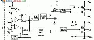
First, let's look at how the microcircuit itself works, and only then we will decide which power supply to assemble from it. First, let's look at how the generator itself works. The figure below shows a fragment of a resistive divider, three op-amps and an RS trigger:
At the initial moment of time, when the supply voltage has just been applied, capacitor C1 is not charged at all inverting inputs of the op-amp there is a zero, and at the non-inverting inputs there is a positive voltage generated by a resistive divider. As a result, it turns out that the voltage at the inverting inputs is less than at the non-inverting inputs and all three op-amps at their outputs generate a voltage close to the supply voltage, i.e. log unit. Since the input R (zero setting) on the trigger is inverting, then for it this will be a state in which it does not affect the state of the trigger, but at the input S there will be a log of one, which sets the output of the trigger to also a log of one and a capacitor Ct through resistor R1 will start charging. In the figure, the voltage at Ct is shown by a blue line, red is the voltage at the DA1 output, green is at the DA2 output, and pink is at the RS trigger output:
As soon as the voltage on Ct exceeds 5 V, a log zero is formed at the DA2 output, and when, continuing to charge Ct, the voltage reaches a value slightly more than 10 volts, a log zero will appear at the DA1 output, which in turn will serve to set the RS trigger to the log zero state. From this moment, Ct will begin to discharge, also through resistor R1, and as soon as the voltage on it becomes slightly less than the set value by dividing the value of 10 V, a log unit will again appear at the output of DA1. When the voltage on the capacitor Ct becomes less than 5 V, a log one will appear at the output of DA2 and turn the RS trigger into the one state and Ct will begin to charge again. Of course, at the inverse output of the RS trigger, the voltage will have opposite logical values. Thus, at the outputs of the RS trigger, levels of log one and zero are formed that are opposite in phase, but equal in duration:
Since the duration of the control pulses IR2153 depends on the charge-discharge rate of the capacitor Ct, it is necessary to carefully pay attention to flushing the board from flux - there should be no leaks from the terminals of the capacitor or from the printed conductors of the board, since this is fraught with magnetization of the core of the power transformer and failure power transistors. There are also two more modules in the chip - UV DETECT
and
LOGIK
.
The first of them is responsible for starting and stopping the generator process, depending on the supply voltage, and the second generates DEAD TIME
, which are necessary to eliminate the through current of the power stage. Next, the logical levels are separated - one becomes the control upper arm of the half-bridge, and the second the lower one. The difference is that the upper arm is controlled by two field-effect transistors, which, in turn, control the final stage, which is “detached” from the ground and “detached” from the supply voltage. If we consider a simplified circuit diagram for connecting the IR2153, it turns out something like this:
Pins 8, 7 and 6 of the IR2153 microcircuit are VB, HO and VS outputs, respectively, i.e. power supply for the upper side control, the output of the final stage of the upper side control and the negative wire of the upper side control module. Attention should be paid to the fact that at the moment of switching on, the control voltage is present at the Q RS trigger, therefore the low-side power transistor is open. Capacitor C3 is charged through diode VD1, since its lower terminal is connected to the common wire through transistor VT2. As soon as the RS trigger of the microcircuit changes its state, VT2 closes, and the control voltage at pin 7 of IR2153 opens transistor VT1. At this moment, the voltage at pin 6 of the microcircuit begins to increase, and to keep VT1 open, the voltage at its gate must be greater than at the source. Since the resistance of an open transistor is equal to tenths of an ohm, the voltage at its drain is not much greater than at the source. It turns out that holding the transistor in the open state requires a voltage of at least 5 volts more than the supply voltage, and indeed it is - capacitor C3 is charged to 15 volts and it is this that allows you to keep VT1 in the open state, since the energy stored in it during this the moment of time is the supply voltage for the upper arm of the window stage of the microcircuit. Diode VD1 at this point in time does not allow C3 to discharge to the power bus of the microcircuit itself. As soon as the control pulse at pin 7 ends, transistor VT1 closes and then VT2 opens, which again charges capacitor C3 to a voltage of 15 V.
Quite often, amateurs install an electrolytic capacitor with a capacity of 10 to 100 μF in parallel with capacitor C3, without even delving into the need for this capacitor. The fact is that the microcircuit is capable of operating at frequencies from 10 Hz to 300 kHz and the need for this electrolyte is relevant only up to frequencies of 10 kHz, and then only on condition that the electrolytic capacitor is of the WL or WZ series - technologically they have small ers
and are better known as computer capacitors with inscriptions in gold or silver paint:
For popular conversion frequencies used in the creation of switching power supplies, frequencies are taken above 40 kHz, and sometimes raised to 60-80 kHz, so the relevance of using an electrolyte simply disappears - even a capacitance of 0.22 μF is already enough to open and hold the SPW47N60C3 transistor open , which has a gate capacitance of 6800 pF. To ease the conscience, a 1 µF capacitor is installed, and allowing for the fact that IR2153 cannot switch such powerful transistors directly, the accumulated energy of capacitor C3 is enough to control transistors with a gate capacitance of up to 2000 pF, i.e. all transistors with a maximum current of about 10 A (list of transistors below in the table). If you still have doubts, then instead of the recommended 1 µF, use a 4.7 µF ceramic capacitor, but this is pointless:
It would be unfair not to note that the IR2153 microcircuit has analogues, i.e. microcircuits with a similar functional purpose. These are IR2151 and IR2155. For clarity, let’s put the main parameters in a table, and then we’ll figure out which of them is best to prepare:
| CHIP | Maximum Driver Voltage | Start supply voltage | Stop supply voltage | Maximum current for charging the gates of power transistors / rise time | Maximum power transistor gate discharge current/fall time | Internal Zener diode voltage |
| IR2151 | 600 V | 7.7…9.2 V | 7.4…8.9 V | 100 mA / 80…120 nS | 210 mA / 40…70 nS | 14.4…16.8 V |
| IR2153 | 600 V | 8.1…9.9 V | 7.2…8.8 V | NOT SPECIFIED / 80…150 nS | NOT SPECIFIED / 45…100 nS | 14.4…16.8 V |
| IR2155 | 600 V | 7.7…9.2 V | 7.4…8.1 V | 210 mA / 80…120 nS | 420 mA / 40…70 nS | 14.4…16.8 V |
As can be seen from the table, the differences between the microcircuits are not very large - all three have the same shunt zener diode power supply, the start and stop supply voltages are almost the same for all three. The difference lies only in the maximum current of the final stage, which determines which power transistors and at what frequencies the microcircuits can control. Oddly enough, the most hyped IR2153 turned out to be neither fish nor fowl - its maximum current of the last driver stage is not standardized, and the rise-fall time is somewhat prolonged. They also differ in cost - IR2153 is the cheapest, but IR2155 is the most expensive. The generator frequency, it is the conversion frequency (no need to divide by 2) for IR2151 and IR2155 is determined by the formulas given below, and the frequency of IR2153 can be determined from the graph:
In order to find out which transistors can be controlled by the IR2151, IR2153 and IR2155 microcircuits, you should know the parameters of these transistors. The greatest interest when connecting a microcircuit and power transistors is the gate energy Qg, since it is this energy that will influence the instantaneous values of the maximum current of the microcircuit drivers, which means a table with transistor parameters will be required. SPECIAL HERE
Attention should be paid to the manufacturer, since this parameter differs from different manufacturers. This is most clearly seen in the example of the IRFP450 transistor. I understand perfectly well that for a one-time production of a power supply, ten to twenty transistors are still too much, nevertheless, I posted a link for each type of transistor - I usually buy there. So click, see the prices, compare with retail and the likelihood of buying lefty. Of course, I’m not saying that on Ali there are only honest sellers and all the goods are of the highest quality - there are a lot of scammers everywhere. However, if you order transistors that are produced directly in China, it is much more difficult to run into crap. And it is for this reason that I prefer STP and STW transistors, and I don’t even hesitate to buy them from disassembly, i.e. BOO.
| POPULAR TRANSISTORS FOR PULSE POWER SUPPLY | |||||||
| NAME | VOLTAGE | CURRENT | RESISTANCE | POWER | GATE CAPACITY | Qg (MANUFACTURER) | FRAME |
| NETWORK (220 V) | |||||||
| IRFBC30 | 600V | 3.6A | 1.8 Ω | 100W | 660pF | 17…23nC (ST ) | |
| IRFBC40 | 600V | 6.2A | 1 Ω | 125W | 1300pF | 38…50nC (ST ) | |
| IRF740 | 400V | 10A | 0.48 Ω | 125W | 1400pF | 35…40nC (ST ) | |
| IRF840 | 500V | 8A | 0.85 Ω | 125W | 1300pF | 39…50nC (ST ) | |
| STP8NK80Z | 800V | 6A | 1.3 Ω | 140W | 1300pF | 46nC (ST ) | |
| STP10NK60Z | 600V | 10A | 0.75 Ω | 115W | 1370pF | 50…70nC (ST ) | |
| STP14NK60Z | 600V | 13A | 0.5 Ω | 160W | 2220pF | 75nC (ST ) | |
| STP25NM50N | 550V | 22A | 0.14 Ω | 160W | 2570pF | 84nC (ST ) | |
| IRFB18N50K | 500V | 17A | 0.26 Ω | 220W | 2830pF | 120nC (IR) | |
| SPA20N60C3 | 650V | 20A | 0.19 Ω | 200W | 2400pF | 87…114nC (IN) | |
| STP17NK40Z | 400V | 15A | 0.25 Ω | 150W | 1900pF | 65nC (ST ) | |
| STP8NK80ZFP | 800V | 6A | 1.3 Ω | 30W | 1300pF | 46nC (ST ) | |
| STP10NK60FP | 600V | 10A | 0.19 Ω | 35W | 1370pF | 50…70nC (ST ) | |
| STP14NK60FP | 600V | 13A | 0.5 Ω | 160W | 2220pF | 75nC (ST ) | |
| STP17NK40FP | 400V | 15A | 0.25 Ω | 150W | 1900pF | 65nC (ST ) | |
| STP20NM60FP | 600V | 20A | 0.29 Ω | 45W | 1500pF | 54nC (ST ) | |
| IRFP22N60K | 600V | 22A | 0.24 Ω | 370W | 3570pF | 150nC(IR) | |
| IRFP32N50K | 500V | 32A | 0.135 Ω | 460W | 5280pF | 190nC(IR) | |
| IRFPS37N50A | 500V | 36A | 0.13 Ω | 446W | 5579pF | 180nC(IR) | |
| IRFPS43N50K | 500V | 47A | 0.078 Ω | 540W | 8310pF | 350nC(IR) | |
| IRFP450 | 500V | 14A | 0.33 Ω | 190W | 2600pF | 150nC (IR) 75nC (ST ) | |
| IRFP360 | 400V | 23A | 0.2 Ω | 250W | 4000pF | 210nC(IR) | |
| IRFP460 | 500V | 20A | 0.27 Ω | 280W | 4200pF | 210nC(IR) | |
| SPW20N60C3 | 650V | 20A | 0.19 Ω | 200W | 2400pF | 87…114nC (IN) | |
| SPW35N60C3 | 650V | 34A | 0.1 Ω | 310W | 4500pF | 150…200nC (IN) | |
| SPW47N60C3 | 650V | 47A | 0.07 Ω | 415W | 6800pF | 252…320nC (IN) | |
| STW45NM50 | 550V | 45A | 0.1 Ω | 417W | 3700pF | 87…117nC (ST) | |
As is known, the dynamic properties of a field-effect transistor are most accurately characterized not by the value of its parasitic capacitances, but by the total gate charge - Qg. The value of the Qg parameter mathematically connects the pulse current of the gate with the switching time of the transistor, thereby providing the developer with the opportunity to correctly calculate the control unit. For example, for an IRF840 field-effect transistor with a drain current Is = 8 A, a drain-source voltage Uds = 400 V and a gate-source voltage Ugs = 10 V, the total gate charge is Qg = 63 nC. At a constant gate-source voltage, the gate charge decreases with increasing drain current Is and with decreasing drain-source voltage Ugs. Let us calculate the parameters of the control circuit, provided that it is necessary to achieve a turn-on time of the transistor ton = 120 ns. To do this, the driver control current must have the value:
Ig = Qg / ton = 63 x 10-9 / 120 x 10-9 = 0.525 (A) (1)
When the amplitude of the control voltage pulses at the gate is Ug = 15 V, the sum of the output resistance of the driver and the resistance of the limiting resistor should not exceed:
Rmax = Ug / Ig = 15 / 0.525 = 29 (Ohm) (2)
Let's calculate the output impedance of the driver stage for the IR2155 chip:
Ron = Ucc / Imax = 15V / 210mA = 71.43 ohms Roff = Ucc / Imax = 15V / 420mA = 33.71 ohms
Taking into account the calculated value according to formula (2) Rmax = 29 Ohm, we come to the conclusion that with the IR2155 driver it is impossible to achieve the specified speed of the IRF840 transistor. If a resistor Rg = 22 Ohm is installed in the gate circuit, the turn-on time of the transistor will be determined as follows:
REon = Ron + Rgate, where RE is the total resistance, Rout is the output resistance of the driver, Rgate is the resistance installed in the gate circuit of the power transistor = 71.43 + 22 = 93.43 ohms; Ion = Ug / REon, where Ion is the opening current, Ug is the value of the gate control voltage = 15 / 93.43 = 160mA; ton = Qg / Ion = 63 x 10-9 / 0.16 = 392nS The turn-off time can be calculated using the same formulas: REoff = Rout + Rgate, where RE is the total resistance, Rout is the driver output resistance, Rgate is the resistance installed in the circuit power transistor gate = 36.71 + 22 = 57.71 ohms; Ioff = Ug / REoff, where Ioff is the opening current, Ug is the value of the gate control voltage = 15 / 58 = 259mA; toff = Qg / Ioff = 63 x 10-9 / 0.26 = 242nS To the resulting values, it is necessary to add the time of the transistor’s own opening and closing, resulting in the real time ton being 392 + 40 = 432nS, and toff 242 + 80 = 322nS. Now all that remains is to make sure that one power transistor has time to close completely before the second one begins to open. To do this, add ton and toff to get 432 + 322 = 754 nS, i.e. 0.754 µS. What is it for? The fact is that any of the microcircuits, be it IR2151, or IR2153, or IR2155, has a fixed DEAD TIME
, which is 1.2 µS and does not depend on the frequency of the master oscillator.
The datasheet mentions that Deadtime (typ.) 1.2 µs, but it also contains a very confusing figure from which the conclusion suggests itself that DEAD TIME
is 10% of the duration of the control pulse:
To dispel doubts, the microcircuit was turned on and a two-channel oscilloscope was connected to it:
The power supply was 15 V, and the frequency was 96 kHz. As can be seen from the photograph, with a scan of 1 µS, the duration of the pause is quite a bit more than one division, which exactly corresponds to approximately 1.2 µS. Next we reduce the frequency and see the following:
As can be seen from the photo, at a frequency of 47 kHz, the pause time practically did not change, therefore the sign stating that Deadtime (typ.) 1.2 µs is true. Since the microcircuit was already working, it was impossible to resist one more experiment - lowering the supply voltage to make sure that the generator frequency would increase. The result is the following picture:
However, expectations were not met - instead of increasing the frequency, there was a decrease in frequency, by less than 2%, which can be generally ignored and noted that the IR2153 microcircuit keeps the frequency quite stable - the supply voltage has changed by more than 30%. It should also be noted that the pause time has increased slightly. This fact is somewhat pleasing - as the control voltage decreases, the opening and closing time of the power transistors increases slightly and increasing the pause in this case will be very useful. It was also found that UV DETECT
copes with its function perfectly - with a further decrease in the supply voltage, the generator stopped, and with an increase, the microcircuit started again.
Now let’s return to our mathematics, based on the results of which we found that with 22 Ohm resistors installed in the gates, the closing and opening time is equal to 0.754 µS for the IRF840 transistor, which is less than the 1.2 µS pause given by the microcircuit itself. Thus, with the IR2155 microcircuit through 22 Ohm resistors it will be quite normal to control the IRF840, but the IR2151 will most likely have a long life, since to close and open the transistors we needed a current of 259 mA and 160 mA, respectively, and its maximum values are 210 mA and 100 ma. Of course, you can increase the resistance installed in the gates of power transistors, but in this case there is a risk of going beyond the DEAD TIME
. In order not to engage in fortune telling on coffee grounds, a table was compiled in EXCEL, which can be taken HERE. It is assumed that the supply voltage of the microcircuit is 15 V. To reduce switching noise and slightly reduce the closing time of power transistors in switching power supplies, either the power transistor is shunted with a resistor and capacitor connected in series, or the power transformer itself is shunted with the same chain. This node is called a snubber. The snubber circuit resistor is chosen with a value 5–10 times greater than the drain-source resistance of the field-effect transistor in the open state. The capacitance of the circuit capacitor is determined from the expression: C = tdt/30 x R where tdt is the pause time for switching the upper and lower transistors. Based on the fact that the duration of the transient process, equal to 3RC, should be 10 times less than the duration of the dead time value tdt. Damping delays the opening and closing moments of the field-effect transistor relative to differences in the control voltage across its gate and reduces the rate of change in voltage between the drain and the gate. As a result, the peak values of the flowing current pulses are smaller and their duration is longer. Almost without changing the turn-on time, the damping circuit noticeably reduces the turn-off time of the field-effect transistor and limits the spectrum of generated radio interference.
Now that we've sorted out the theory a little, we can move on to practical schemes.
The simplest switching power supply circuit based on IR2153 is an electronic transformer with a minimum of functions:
The circuit does not have any additional functions, and the secondary bipolar power supply is formed by two rectifiers with a midpoint and a pair of dual Schottky diodes. The capacitance of capacitor C3 is determined at the rate of 1 μF of capacitance per 1 W of load. Capacitors C7 and C8 are of equal capacity and range from 1 µF to 2.2 µF. The power depends on the core used and the maximum current of the power transistors and theoretically can reach 1500 W. However, this is only THEORETICALLY
, based on the fact that 155 VAC is applied to the transformer, and the maximum current of the STP10NK60Z reaches 10A. In practice, all datasheets indicate a decrease in the maximum current depending on the temperature of the transistor crystal, and for the STP10NK60Z transistor the maximum current is 10 A at a crystal temperature of 25 degrees Celsius. At a crystal temperature of 100 degrees Celsius, the maximum current is already 5.7 A and we are talking specifically about the temperature of the crystal, and not the heat sink flange, and even more so about the temperature of the radiator. Therefore, the maximum power should be selected based on the maximum current of the transistor divided by 3 if it is a power supply for a power amplifier and divided by 4 if it is a power supply for a constant load, such as incandescent lamps. Considering the above, we find that for a power amplifier you can get a switching power supply with a power of 10 / 3 = 3.3A, 3.3A x 155V = 511W. For a constant load we get a power supply 10 / 4 = 2.5 A, 2.5 A x 155V = 387W. In both cases, 100% efficiency is used, which does not happen in nature. In addition, if we assume that 1 µF of primary power supply capacity per 1 W of load power, then we will need a capacitor or capacitors with a capacity of 1500 µF, and such a capacitance must be charged through soft start systems. A switching power supply with overload protection and soft start via secondary power is presented in the following diagram:
First of all, this power supply has overload protection made on the current transformer. Details on current transformer calculations can be found HERE. However, in the vast majority of cases, a ferrite ring with a diameter of 12...16 mm, on which about 60...80 turns are wound in two wires, is quite sufficient. Diameter 0.1…0.15 mm. Then the beginning of one winding is connected to the ends of the second. This is the secondary winding. The primary winding contains one or two, sometimes one and a half turns are more convenient. Also in the circuit, the values of resistor R4 and R6 have been reduced in order to expand the range of the primary supply voltage (180...240V). In order not to overload the zener diode installed in the microcircuit, the circuit has a separate zener diode with a power of 1.3 W at 15 V. In addition, a soft start for secondary power was introduced into the power supply, which made it possible to increase the capacitance of the secondary power filters to 1000 µF at an output voltage of ±80 V Without this system, the power supply would go into protection the moment it was turned on. The principle of operation of the protection is based on the operation of IR2153 at an increased frequency at the moment of switching on. This causes losses in the transformer and it is not able to deliver maximum power to the load. As soon as generation begins through the divider R8-R9, the voltage supplied to the transformer reaches the detector VD5 and VD7 and charging of the capacitor C7 begins. As soon as the voltage becomes sufficient to open VT1, C3 is connected to the frequency-setting chain of the microcircuit and the microcircuit reaches the operating frequency. Additional inductances for the primary and secondary voltages have also been introduced. Inductance on the primary power supply reduces interference created by the power supply and going into the 220V network, and on the secondary power supply it reduces RF ripple on the load. In this version there are two additional secondary supplies. The first is intended to power a twelve-volt computer cooler, and the second is to power the preliminary stages of a power amplifier. Another sub-option of the circuit is a switching power supply with a unipolar output voltage:
Of course, the secondary winding is designed for the voltage that is needed. The power supply can be soldered on the same board without mounting elements that are not on the diagram.
The next version of the switching power supply is capable of delivering about 1500 W to the load and contains soft start systems for both primary and secondary power, has overload protection and voltage for the forced cooling cooler. The problem of controlling powerful power transistors is solved by using emitter followers on transistors VT1 and VT2, which discharge the gate capacitance of powerful transistors through themselves:
Such forcing of the closing of power transistors allows the use of quite powerful specimens, such as IRFPS37N50A, SPW35N60C3, not to mention IRFP360 and IRFP460. At the moment of switching on, the voltage is supplied to the primary power diode bridge through resistor R1, since the contacts of relay K1 are open. Next, the voltage is supplied through R5 to the microcircuit and through R11 and R12 to the output of the relay winding. However, the voltage increases gradually - C10 has a fairly large capacity. From the second winding of the relay, voltage is supplied to the zener diode and thyristor VS2. As soon as the voltage reaches 13 V, it will be enough to pass through the 12-volt zener diode to open VS2. Here it should be recalled that IR2155 starts with a supply voltage of approximately 9 V, therefore, at the time of opening, VS2 will already generate control pulses through IR2155, only they will enter the primary winding through resistor R17 and capacitor C14, since the second group of contacts of relay K1 is also open . This will significantly limit the charging current of the secondary power filter capacitors. As soon as the thyristor VS2 opens, voltage will be applied to the relay winding and both contact groups will close. The first will bypass the current-limiting resistor R1, and the second - R17 and C14. The power transformer has a service winding and a rectifier on diodes VD10 and VD11 from which the relay will be powered, as well as additional power supply to the microcircuit. R14 serves to limit the forced cooling fan current. The thyristors used VS1 and VS2 are MCR100-8 or similar ones in the TO-92 package. Well, at the end of this page, another circuit is still on the same IR2155, but this time it will act as a voltage stabilizer:
The last author's circuit using IR2155 will be an automotive voltage converter circuit in which IR2155 will act as the control element of the midpoint converter. In this circuit, the upper side driver is connected to the supply voltage of the microcircuit and the common wire, which allows it to control the transistor VT6:
As in the previous version, the power transistors are closed by bipolars VT4 and VT5. The circuit is equipped with a soft start of the secondary voltage on VT1. The start is made from the vehicle’s on-board power supply and then the power is supplied by a stabilized voltage of 15 V, vortexed by diodes VD8, VD9, resistor R10 and zener diode VD6. There is another rather interesting element in this circuit - tC. This is heatsink overheat protection that can be used with almost any converter. It was not possible to find an unambiguous name; in common parlance it is a self-restoring thermal fuse; in price lists it is usually designated KSD301. It is used in many household electrical appliances as a protective or temperature-regulating element, since they are produced with different response temperatures. This fuse looks like this:
As soon as the radiator temperature reaches the fuse cut-off limit, the control voltage from the REM point will be removed and the converter will turn off. After the temperature drops by 5-10 degrees, the fuse will be restored and supply control voltage and the converter will start again. The same thermal fuse, or thermal relay, can also be used in network power supplies by monitoring the temperature of the radiator and turning off the power, preferably low-voltage, going to the microcircuit - the thermal relay will work longer this way. You can buy KSD301 HERE. VD4, VD5 - fast diodes from the SF16, HER106, etc. series. Overload protection can be introduced into the circuit, but during its development the main emphasis was on miniaturization - even the soft start unit was a big question. The manufacture of winding parts and printed circuit boards are described on the following pages of the article. Well, at the end of the day there are several circuits of switching power supplies found on the Internet. Scheme No. 6 taken from the SOLDERING IRON website:
The protection is organized on the voltage drop across resistors R10-R11, but it monitors the current flowing only through the transient VT4. In principle, nothing terrible, but it is still advisable to keep an eye on both transients. As mentioned above, the large capacity of the voltage booster does not make sense and the author used a 0.68 mF capacitor (C7).
The following network converter circuit is notable for the fact that the power transformer has an additional winding to power the IR2153 microcircuit itself. Inductance L3 has also been introduced, reducing shock processes in the transformer:
In the next power supply on the self-clocked driver IR2153, the capacitance of the boost capacitor is reduced to a minimum of 0.22 μF (C10). The microcircuit is powered from an artificial midpoint of the power transformer, which is not important. There is no overload protection; the shape of the voltage supplied to the power transformer is slightly corrected by the inductance L1:
While selecting diagrams for this article, I came across this one. The idea is to use two IR2153 in a bridge converter. The author’s idea is quite clear - the output of the RS trigger is fed to the input Ct and, according to the logic, control pulses of opposite phase should be generated at the outputs of the slave microcircuit. The idea intrigued me and an investigative experiment was carried out on the topic of testing its functionality. It was not possible to obtain stable control pulses at the outputs of IC2 - either the upper driver or the lower one was working. In addition, the pause phase DEAD TIME
, on one microcircuit relative to another, which will significantly reduce the efficiency and the idea was forced to be abandoned.
The distinctive feature of the next power supply on the IR2153 is that if it works, then this work is akin to a powder keg. First of all, the additional winding on the power transformer to power the IR2153 itself caught my eye. However, there is no current-limiting resistor after diodes D3 and D6, which means that the fifteen-volt zener diode located inside the microcircuit will be VERY heavily loaded. One can only guess what will happen if it overheats and undergoes thermal breakdown. The overload protection on VT3 bypasses the time setting capacitor C13, which is quite acceptable.
This switching power supply circuit is capable of developing quite a lot of power, since after the output stage of the microcircuit, additional emitter followers are installed on bipolar transistors, which actually control the gates of the power transistors. In this option, the maximum power of the converter will already depend on the maximum current of bipolar transistors and the maximum current of power field switches. Since the consumption for switching power transistors has increased, the capacity of the voltage boost capacitor has been increased to 2.2 μF.
The last acceptable version of the power source circuit on the IR2153 does not represent anything unique. True, for some reason the author too reduced the resistance of the resistors in the gates of the power transistors and installed zener diodes D2 and D3, the purpose of which is very unclear. In addition, the capacitance C11 is too small, although it is possible that we are talking about a resonant converter.
There is another option for a switching power supply using IR2155 and specifically for controlling a bridge converter. But there the microcircuit controls power transistors through an additional driver and matching transformer and we are talking about induction melting of metals, so this option deserves a separate page, and everyone who understands at least half of what you read should go to the page with PRINTED BOARDS.
I strongly recommend reading: CALCULATIONS OF PULSE POWER SUPPLY SUPPLY IN EXCEL
VIDEO INSTRUCTIONS FOR YOURSELF ASSEMBLY OF A SWITCH POWER SUPPLY BASED ON IR2153 OR IR2155
A few words about the manufacture of pulse transformers:
How to determine the number of turns without knowing the grade of ferrite:
A few nuances when assembling the power supply on the IR2153:
The last one will be a video on how to make a power supply on IR2155, and with stabilization of the output voltage. The video describes in detail how stabilization is carried out, and provides options for organizing the stabilization of the output voltage or current.
I bought thermal tape on Aliexpress; to be specific, the seller is listed here.
Site administration address
Possible changes
The oscillator frequency is controlled by a potentiometer and covers the range from 10 kHz to 100 kHz, duty cycle 50%.
Useful: Do-it-yourself home audio amplifier for speakers
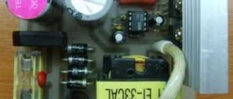
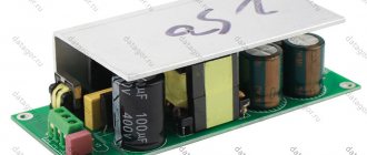
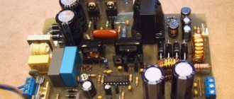
Ready power supply for IR2153
Naturally, other MOSFETs or IGBTs can be used in the above circuits. Don't forget that transistors require a large heatsink. you can follow the link.
Use and abuse of IR2153 for feeders up to 1.5kW
This point will be discussed in the IR2153 manual, or better yet, it will be theoretically presented as a basis for constructing various switching power supplies. IR2153 This is a high voltage driver with an internal oscillator. This allows the implementation of switching power supplies up to 1.5 kW based on half-bridge circuits with minimal circuitry.
Considering what they say in the article IR2153 and in the title there are also models IR2151 and IR2155 hey
I made a table that highlights the main differences,
They are interchangeable as long as the powers involved aren't high, but as long as we don't go below 300W there's nothing stopping you from using one of the three indiscriminately, unless you want to take the risk you should still get the strongest IR2155.
In the article I also explain what these differences are and when to use a template instead of another.
There are two variants of the same integrated one, they differ only in the presence of a diode from the boost voltage:
Block diagram of IR2153
functional diagram of IR2153D with internal diode D1
The figure below shows the input stage consisting of three op-amps and a flip-flop SR:
At first I did not notice, ragionandoci some mental fog disappeared and I realized where I had seen a similar circuit, turns corners even at a distance of 50 years continue to use 555!!
Block diagram 555
Initially, when you apply voltage, C1 discharges, and the op-amp's inverting input is zero, and the non-non-inverting input has a positive voltage, represented by a resistive divider. The result is that all three have an output voltage at logic level one. Since the R input is active at zero level there will be no effect on the output state, but the S input will set the output Q of the flip-flop, which C1 begins to charge through resistor R1.
The voltage path at Ct is shown by the blue line, red is at the voltage output of OP1, green is at the output of Op2, Rose, the Q output is from the flip-flop, and the Q output mustard is rejected.
As soon as the voltage on Ct exceeds 5 Output V of OP2 to zero, continuing to load C1, the voltage reaches a value slightly higher than 10 Volts and this time the output of OP1 tends to zero, which, in turn, leads to zero output Q trigger signal. From this point C1 begins to discharge through resistor R1, and as soon as the voltage on it is a little less than 10V l'Uscita Na1 returns 1. When the voltage on capacitor Ct becomes less than 5V, the output Op2 will reset the flip-flop and restart charging Ct.
The chip contains two additional UV DETECTION
e
LOGIC.
The first of these is responsible for enabling the charging process on C1 only when a certain power supply voltage is exceeded and generates the second delay pulses, which are necessary to prevent both ends from being conductive, at the same time by short-circuiting the power supply through the power stage. Next is the separation of the logic levels for the middle and upper decks to the lower one.
Let's look at a typical simplified circuit from an IR2153:
I pin 8, 7 e 6, respectively, is the output of VB, HO and VS, that is, power control is the upper branch (VB), final stage piloting (HO) and the negative upper branch of the control module (VS) . Note the fact that when the lower branch is active, diode D1 begins to load C3 fact with T2 in conduction state, the capacitor is practically connected to ground. Once the output signals change state, T2 isolates, and HO through T1 enters the conduction state. At this point, the voltage across VS begins to increase to the level of total positive power, provided that T1 under these conditions has a resistance of tenths of ohms.
It turns out that keeping a conductive transistor requires a gate voltage at least 8 volts higher than the supply voltage. It provides exactly C3 loaded with 15 volts, which allows T1 to remain conductive, thanks to the energy stored in it when T2 was conductive thanks to D1. In this phase, the same diode does not allow the capacitor to be connected to the same power supply. As soon as the pin on the pulse control 7 completes the transistor T1 opens and closes in its place T2, the capacitor C3 is again charged to a voltage of 15 V. The value of C3 largely depends on the time at which it conducts T1. You should avoid using electrolyte for operating frequencies above 10KHz, while such an Ic is capable of operating from 10Hz to 300KHz.
Working from almost 40 to 80kHz when used, 220nF will be enough power to make sure you choose the 1uF value. Generator frequency, This can be determined from this graph in the integrated data, for convenience I have attached a copy.
Selecting the appropriate MOSFET
In the table below I summarize the characteristics of the most commonly used MOSFET that I found around this integrated one. Useful in case you have to look for an equivalent in case of breaks, sifting through the table we can choose between the models at our disposal which, although not exactly equivalent, goes well in any case.
It can be used to power a design from scratch.
Calculation of relative gate resistance
As is known, the dynamic properties of a field-effect transistor are not characterized more accurately by the value of its parasitic capacitances, but by the total charge of the gate Qg-. The value of the Qg parameter is mathematically related by the pulse current to the switching time gate of the transistor, which allows the developer to correctly calculate the control unit. Take for example, IRF840 MOSFETs are very common and present in the table.
With current drain Id = 8 A, drain-source Vds = 400 V and gate-source voltage Vgs = 10 V, gate charge Qg is = 63 nC.
It should be clarified that with the same Vgs, the gate charge decreases with increasing current Id and the drain charge with decreasing voltage Vds, in the calculations it is clear that both voltages are constant for good they accept the value specified by the manufacturer, small changes do not affect the final result of the calculations. We will calculate the parameters of the control circuit, provided that it is necessary to achieve a transistor turn-on time of t = 120 ns. To do this, the driver's current control must have the value:
T = Qg / t = 63 x 10-9 / 120 x = 10-9 0.525 (A) (1)
When the amplitude of the control voltage pulses at the gate is Vg = 15 V, the sum of the driver output resistance and the resistance of the limiting resistor should not exceed:
Rmax = Vg / Ig = 15 / 0.525 = 29 (ohm) (2)
Let's calculate the output resistance of the cascade at the driver output for the IR2155 chip:
Ron = Vcc / Imax = 15V / 210mA = 71.43 ohms Roff = Vcc / Imax = 15V / 420mA = 35.71 ohms
Taking into account the value calculated by formula (2) Rmax = 29 ohms, we come to the conclusion that the specified speed of the IRF840 transistor cannot be obtained by the IR2155 driver. If in the gate circuit, the resistor Rg is set = 22 ohms, the ignition time of the transistor is determined as follows:
Reon = Rg + RF, dove
RE = impedance
Rf = driver output impedance,
Rg = external gate resistance of the power transistor
Reon = + 71.43 = 93.43 ohms; Ion = Vg/RE, dove
Ion = drive current
Vg = gate control voltage value
Ion = 15 / 93.43 = 160mA; t = Qg / Ion = 63 x 10-9 / 0.16 = 392 nS Sleep time can be calculated with the above formulas:
REoff = Rf + Rg = 35.71 + 22 = 57.71 ohms;
Ioff = Vg / Reoff = 15/58 = 259mA
Tsr = Qg / Ioff = 63 x 10-9 / 0.26 = 242nS In order to get the real time value, you need to add the time that the transistor physically uses to move from one stage to another, and this is 40ns for by condition and 80ns for this will be turned off in real time
tone 392 + 40 = 432nS, e Toff 242 + 80 = 322nS.
Now it remains to be determined whether the power transistor will have time to completely close before a second start to open. Tal fine, we add Ton and TOff to get 432 + 322 = 754 nS, which is equivalent to 0.754 µS.
From the data it is clear that DEAD TIME
IR2151 cannot be used as it is 0.6 µS.
The datasheet says Deadtime (advice.) This is fixed and depends on the model, but there is also a very awkward figure it comes out of that is DEAD TIME
is 10% of the control pulse duration:
To dispel doubts, I did some tests with a two-channel oscilloscope on the main circuit to see what happened, a child's curiosity for things I've never lost, this is the result:
The power was 15 V, and the frequency was 95 kHz. As you can see in the photos, with a sweep of 1 µS, the pause length is slightly longer than one division, which corresponds exactly to 1.2 µS. Additionally, frequency reduction can be considered as follows:
As you can see in the picture of the 47 kHz frequency, the pause time practically does not change, then the part that says Dead Time (advice) 1.2 mS is correct. Since the circuits were already functioning, it was impossible to hold back another experiment, reducing the supply voltage so that the generator frequency did not increase. The result is the following image:
however, the expectations were not met; instead of an increase in frequency, I witnessed a decrease in frequency. Fortunately, however, the change is less than 2%.
The values are insignificant given changes in supply of more than 30%. It should also be noted that the pause time is slightly increased. This fact is quite good when the control voltage is reduced slightly by changing the opening and closing time of the power transistors and increasing the gap in this case is very useful. Please note that UV DETECTION
with a function that blocks the generator in case of excessive reduction of the power supply, and then re-activates the chip when it goes beyond the minimum level. Now back to our example, with a gate resistor of 22 ohms closing and opening another 0.754 µS con of the IRF840, this value is less than the 1.2 us pause typical of the chip itself. so with IR2155 and IR2153 through 22 ohm resistors can control the IRF840, but of course the IR2151 will be discarded and also the dead time is too low because the transistors need to be aware of 259m and 160mA while the IR2151 has the maximum value 210 m and 100 mom. Obviously, it is possible to increase the resistance set at the gate of the power transistor, but in this case there is a risk of exceeding the dead time limits. In order to reduce the switching noise of power transistors in a switching power supply, a shunt resistor is used in series with a capacitor in parallel with the transformer winding. This unit is called a damper. The suppression range resistor is selected by estimating 5-10 times the drain-source resistance of the MOSFET.
The capacitance is determined by the expression: C = TDT / 30 x R TDT is the turn-off time of the upper and lower transistor.
Based on the fact that the duration of the transition is 3RC, it should be 10 times less than the duration of the TDT. The damper delays the opening and closing moments of the field-effect transistor control voltage fluctuations in relation to its door and reduces the rate of change of voltage between the drain and the gate. As a result, the peak values of the pulsed current pulses are negligible and their service life is longer. With almost no change in stepper period, the damping circuit significantly reduces the FET turn-off time and limits the spectrum of noise generated. You can find it in a position drawn indifferemtemente or directly parallel to the trasgormatore winding, the differences between these two configurations are so marginal as to be considered interchangeable in practice.
Here are some practical models seen around.
Almost none of the following patterns for the number of turns in transformers are specified, because they must be calculated depending on the characteristics of the transformer itself, and also because in most cases the patterns that I have found are not defined. The simplest switching power supply with IR2153 This is an electronic transformer with minimal functions:
In circuit 1, there are no additional functions, and the secondary is formed by two bipolar supply rectifiers consisting of a pair of double Schottky diodes. 220 µF capability Output to bridge is calculated with the empirical formula of 1 µF per load watt. In this case, a 100W stereo amplifier is used for each channel. Two capacitors 2 and 2 on the primary winding of the transformer are placed in the range from 1 2 and 2.
The power depends on the transformer core, and the maximum current of power transistors can, in theory, reach 1500 watts. in practice, in this circuit the maximum current depends on the temperature of the STP10NK60Z transistor, the maximum current is 10 A If you only have 25 degrees. When the silicon salt temperature of 100 degrees is reduced to 5.7A, and talk about the temperature of the silicon, and not the temperature of the radiator. So the maximum power should be chosen according to the transistor current divided by 3 if you are feeding a power amplifier and divided by 4 if one is feeding a constant load such as incandescent lamps. In this case, it is theoretically possible to drive the amplifier
10/3 = 3.3a 3.3a x = 155V 511W totali.
With a constant load of 10/4 = 2.5 A 2.5 A x = 155V 387W.
From the calculations reference is made to a fixed voltage of 155V, where does it come from this value? This comes from the effective voltage across the smoothing capacitor at maximum power, the value is empirical, but, It is not very different from the real value and allows us to simplify our lives without deviating too much from the real one.
In both cases the theory is 100% yield, which cannot be achieved.
also, wanting to get a maximum power of 1500W given the need for 1uF of primary power supply capacitance for every watt of power on the load, it needs one or more capacitors to get to 1500uF in total and loading them should be a soft start so as not to jump the counter on each switch.
more power and current protection in circuit 2:
This is realized by overload protection thanks to the current transformer. In most cases, a ferrite ring with a diameter of 12 and 16 mm is used, which encloses 60 and 80 bifilar coils of insulated wire with a diameter of 0.1 mm. In order to form a central tap winding for the secondary. The primary winding is made by winding from one to two coils. Sometimes for convenience and this makes a turn and half, when it comes into function, it reduces the power of the integrated circuit resulting in, thanks to internal protection, stopping the final driving. After scaricatosi electrolyte, the SCR is turned off and the reforms of the right to return the power to run the final regular ones. Two 62K resistors in parallel allow feeding integrated with good primary power supply (180 ... 240V). In order not to overload the internal Zener diode if it uses the external one of the 1.3 W 15 V. An additional circuit on the base around the lower transistor allows a gradual start at a lower frequency, until the full charge of the ± 80 V 1000 µF capacitors.
With a 330K-4k7 divider and the diodes connected to it are loaded initially from the electrolytic 4U7, this is the gate voltage of the transistor which increases the power of the generator, enough time to charge the capacitors too without overloading the ferrite transformer.
After this time, the island transistor and the integrated one operate back at its operating frequency.
The presence of a snubber network eliminates most of the interference caused by the feeder.
Another option for a switching power supply, capable of providing a load of 1500 W, contains a soft start system for the main power supply while the secondary ones have overload protection. It also creates voltage for the fan to force ventilation of the cooling fin. The problem of quickly turning off the power transistor is solved using two BD138 transistors; they discharge the gate capacitance of the MOSFET with extreme simplicity.
Such a system allows the use of relatively powerful elements such as IRFPS37N50A, SPW35N60C3, not to mention IRFP360 and IRFP460. At the moment of the primary ignition voltage on the diode bridge, power flows through a 360 ohm resistor, since the relays open. Also, the voltage across the 47K resistor is used for the chip, simultaneously using two resistors 33 and 360 which relate to the FAN terminal and the relay winding. With them, the capacitor is charged gradually from 100uF since the second part of the relay winding is part of the zener diode and only this voltage reaches 13V. This will cause SCRs that excite the relay. Here you must remember that the IR2155 already starts working with a supply voltage of approximately 9 V, then when the relay is energized it already works by generating control pulses to drive the primary.
Piloting what happens at reduced power shows that when the relay is open it passes through a 360 resistor. It is very important that the trick is to limit the charging current of the secondary power supplies of the filter capacitors. After the relay coil is energized by the thyristor, its contacts are shunted as limiting resistors. The transformer has additional windings to supply the cooling fan (FAN), its resistance is current limiting.
Lately I've been needing a low voltage regulator, but starting with a high starting voltage, below is one elegant solution to this problem, MOSFET T2 is operated as if it were a diode, when you raise the voltage quickly find diodes that can handle high currents , of course, more expensive than a regular MOSFET.
circuit 5 using IR2155 for the amplifier voltage circuit. In this circuit, the high driver is connected to the supply voltage:
As in the previous version, the power transistors are connected with two BD140s. Initially, part of the edge of the car battery with 12V, and then the supplied voltage is stabilized at 15 V through additional voltage suppression diodes, a limiting resistor and a built-in zener diode to stabilize the supply voltage. Not present in the diagram there is a thermal switch that must be fixed in the fins, it will stop the REM voltage when the integrated is turned off. These diodes should be fast fast series SF16, HER106, etc.
With this I think I have clarified many aspects of this family of integrated ones, but as a final treatment, put the adapter I use for my 200+200W amplifier, implemented using a transformer removed from the computer power supply, saved from the landfill.
There is no unique addition in the diagram and the network consisting of a 100 ohm damping resistor with a series capacitor of 100 pF in parallel with each diode on the secondary.
This subsequent modification also makes it suitable for classic linear amplifiers.
It has a soft start EMI filter and overabsorption protection, many of the passive components of the original power, why look elsewhere for what I had on hand?
I purposely didn't explain this last diagram to see if what was said in the article is actually good for anything.
AMILCARE Greetings
| VOTE |
DIY crafts for car enthusiasts
Today we’ll talk and look at a common switching power supply circuit built on the IR2153 chip.
So, we have a switching power supply circuit that is powered by 220 volts and, say, at the output it has some voltage to power something, that is, some kind of amplifier, or some other design.
At the input we have 220 variables, it goes to filter L1 with film capacitors C1 and C2, but this inductor can be removed from the circuit and simply replaced with jumpers, everything will work fine without it.
Then the voltage is supplied to a full-fledged full-wave diode bridge, I did not use a ready-made diode assembly, but ordinary 1N4007 diodes, 4 diodes were assembled from them into a diode bridge, on the diode bridge the voltage is rectified, but not completely rectified, because there still remains some then the half-wave, this sine goes to the smoothing capacitor, in this case there are 100 microfarads 400 volts.
A smoothing capacitor, if you measure it with a multimeter when voltage is applied to it, the voltage will be slightly more than, say, 220 volts, maybe 250-280 volts. What is this connected with? - this capacitor is charged to its amplitude value, then after the smoothing capacitor, the voltage is supplied to the circuit.
We have a common minus of the diode bridge, that is, for powering the entire power circuit and for the microcircuit it is IR2153, that is, for the generator.
The microcircuit is powered - plus to the first pin, minus to the fourth pin. The microcircuit is powered through the chain, R1, VD3, smoothing capacitor C4, which smoothes out interference from the resistor and this entire chain so that the microcircuit works normally.
When connecting and assembling the entire circuit, use the necessary multimeter to check the terminals on the microcircuit 1 + and 4 leg minus, the voltage should be around 15 volts, then the microcircuit will work normally and generate pulses.
Next, between the 8th and 6th legs of the microcircuit there is a film capacitor (C6) of 220 nanofarads, in general the capacitance of this capacitor is selected based on the frequency of the generator, that is, in this case the frequency of the generator is in the region of 47-48 kilohertz, the capacitor can be 0.2 microfarad and 0.47 and 0.68 even one microfarad, that is, here this capacitor is not particularly critical.
This microcircuit operates at a frequency of 47-48 kilohertz, the chain that provides this frequency is a resistor R2 - 15K and a film or ceramic capacitor (C5) of one nanofarad or you can put 820 picofarads.
Pin 5 and pin 7 of the microcircuit generate rectangular control pulses, which through resistors R4 and R3 are supplied to the gates of powerful field-effect transistors, that is, these resistors are needed so as not to accidentally burn the transistors.
For example, a pulse arrives at the gate of a powerful field-effect transistor, then through a ballast capacitor (C7) at 220 nanofarads 400 volts to the primary winding of transformer T1.
As for the transformer , the transformer was taken from a computer power supply.
It needs to be modified a little, that is, desoldered, disassembled, put in boiling water to melt the glue that glues the ferrite or heat it with a soldering hairdryer, put on some gloves so as not to burn your hands and slowly halve and wind up all the windings of this transformer.
Based on the fact that I needed to get around 25 volts at the output, the primary winding with a 0.6 millimeter wire in two cores is wound entirely 38 turns. Each layer was insulated with tape, that is, a winding layer, a layer of insulation, then from top to bottom we again wound everything in one direction, insulated everything and wound the secondary winding.
The secondary winding is 7 cores, the same wires are 0.6 millimeters long and we wind them in the same direction - this is very important, for those who are starting to understand switching power supplies, we wind them all in the same direction.
Just 7 or 8 turns of the secondary winding and then we glue the whole thing back together and put all the ferrite back in place.
The transistors are installed on a small heat sink, this is quite enough for a load somewhere around 100 watts. Two transistors are secured through heat-conducting pads and thermal paste.
Now we will plug it all into the network, take a multimeter and measure the output voltage.
But there is still such a moment, before starting the power supply, we do everything sequentially, that is, we take a 100 watt 220 volt light bulb and connect our power supply through the light bulb, if the light bulb does not light up or the spiral flares up slightly, then the capacitor is charged and everything seems to be fine, You can carefully check our voltage at the output.
If, for example, the light is on, then there are already some mistakes in the circuit, either it’s not soldered somewhere, or there’s snot somewhere on the board, or some component is faulty. So, before assembling, take good parts.
We turn on the multimeter in the mode of measuring a constant voltage of 200 volts and measure at the output our voltage gives me 29 volts
I would like to say that this is my first design, that is, I assembled it the same way as a novice radio amateur who is afraid to assemble his first and switching power supplies, and resorts more to a network transformer.
Archive for the article, you can.
Author; Tumin Igor
Popular;
- Powerful, regulated power supply for lm317
- Garage power supply for repair work
- A simple laboratory power supply made from an old computer power supply.
- How to charge a battery without a charger, diagrams
- Universal power supply 0-30 V with current adjustment from 0-3 A
- Boost converter, DIY circuit
- Simple power supply for the garage
- Powerful charger for any battery
Power supply 1000 Watt on IR2153. Part 1.
What can be done on the basis of a very powerful step-down power supply? a lot of things and the starter-charger is one of these devices. Modern starting and charging devices cost a lot of money - on average 8-10,000 rubles.
To start, you need currents above 100 Amperes; the starter itself, very briefly at the moment of starting, can consume about 230-250 Amperes, taking into account the fact that the battery itself will work in compatibility with the charger, then in principle such currents are not needed.
The basis of any charger is the power supply. A small calculation. How powerful must the power supply be to deliver current above 100 Amps? it turns out to be almost a welding machine, except that welders have a voltage 3-4 times higher than the voltage needed to start the starter. Physics 8th grade - 12Voltx100 Ampere - a total of 1200 watts of power. Imagine a network, iron transformer with such power. It will be large in size and weight, which is not very convenient from the point of view of transportation. But here pulse circuits come to the rescue.
Circuits such as law have electronic filling and consist of numerous individual units that work together. This solution allows you to dramatically reduce the size and weight of the device. Our circuit is based on the popular half-bridge driver IR2153; dozens of circuits have been created based on this chip, but ours differs from all others in its circuit design and output power.
Main components of the circuit.
1) Input block. Mains filter, rectifier and smoothing capacitance 2) Pulse generator and driver for controlling power transistors 3) power transistors and transformer 4) Output block - rectifier, filter 5) Soft start system 6) Protection system
All these nodes work together, making our power supply very reliable and quite powerful.
The circuit was assembled, to be honest, for other purposes, or rather to power powerful low-frequency amplifiers, but nothing prevents us from getting 12-14 Volts at the output. The circuit works in a fairly simple way - 220 Volt mains power is supplied through a filter to a rectifier in the form of a ready-made 8 Ampere diode bridge, where alternating current is converted into direct current, then the rectified power is smoothed out by powerful capacitors 400 Volt 470 µF each, to obtain higher power it is worth using capacitors of larger capacity, for example 2x680 uF 400 Volt. The ideal ratio is 1 watt of power 1uF.
My unit has a calculated power of 1000 watts, but this is not the limit, without any problems you can get 1300 and 1500 watts, although experts say that for half-bridge circuits such powers are not the best option; to obtain higher power, they rightly use the full topology bridge.
The microcircuit (also known as the master oscillator) is powered through a 47 kOhm 2 Watt limiting resistor (it will heat up during operation and this is normal). The microcircuit generates pulses with a frequency of 42 kHz, then the pulses are sent to the driver, which is assembled on complementary pairs BD140/139 with only 4 transistors, by the way, our analogue is KT815G (BD139), KT814G (BD140).
The driver controls powerful field-effect transistors 20N60 - these are N-channel high-voltage transistors with a current of 20 Amps in a TO-220 package - they are enough for 1000 Watts of output power.
Well, then everything is the same as in other power supplies - a power transformer, a rectifier, and a filter, which consists of chokes, and after them smoothing capacitors.
Continued >>