The sound when playing a radio in a car will be more powerful if you install sound amplifiers. They are sold in hardware stores, but some car enthusiasts make them using special patterns.
The main thing is to observe safety precautions and follow the instructions exactly. This publication will discuss how to make a sound amplifier for speakers. Various methods are given that can be applied at home based on the scientific and technical direction of circuit design.
Device base
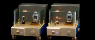
The basis of audio power amplifiers can be any device into which a board can fit. Craftsmen recommend using a column as a body. The power supply and other elements should be installed in it.
Another option for making an amplifier for a car with your own hands is an outdated car radio. The old optical drive is removed from it.
Sometimes only one stereo amplifier remains from the radio, which can not be rebuilt, but used separately.
It is also easy to make a sound amplifier housing with your own hands from thin plywood sheets (up to a centimeter thick), aluminum, double-sided foil fiberglass and other raw materials.
ULF setting
To configure, you need to perform the following steps one by one:
- Inserting the handles of resistors R24, R6 into the middle position.
- Amplifier input shorted to ground.
- Disconnection of terminal transistors.
- Turning on the power supply to the power amplifier circuit.
- Installation of R6 at the output.
- Then the power supply voltage and +/- 15 V are measured.
- Setting the voltage on resistors R29-R30 to 0.55 V using R24.
- This is followed by turning off the power, connecting the terminal transistors, and connecting a 1 A ammeter to the electrical circuit of the VT10 collector.
- Turning on the power and setting R24 collector current to 100-150 mA.
- Measurement of collector current VT11 (it is important that the indicator does not differ from the value of VT10, the maximum difference is 5%).
- The final step is measurement at maximum temperature heating of the radiators of the final transistors (installation is carried out at +35-40°C).
The collector current can be set to 40-200 mA, it all depends on the desired sound quality of the audio amplifiers, operating modes, and radiator parameters.
Speaker protection
This unit does not require configuration if it is assembled correctly. To create a car amplifier with your own hands, you can use radiators that were previously installed in a personal computer. You will also need coolers, since without them there will be strong heating.
They need to be powered using a simple PWM regulator circuit. How to assemble such homemade amplifiers? The steps are performed in the following sequence:
- First, the 2nd converter for the subwoofer channel is assembled. In this case, the previous auto amplifier circuit is used. There are minor changes to how the transformer is wound.
- The two rings are glued together.
- The primary can be left the same. In this case, a different secondary will be needed: the number of cores remains the same, and the turns should be 21, not 15. The output voltage of the converter is plus/minus 70 V.
- For a low-pass filter, you will need to make a winding of eight turns of 0.8 wire.
If we talk about stabilization, it remains identical to that in the car amplifier circuit. A wire winding is also provided to power the protection of the speaker system.
Based on Anthony Holton's design
To assemble a subwoofer amplifier in a car, you need to follow these instructions:
- It is recommended to start assembling an amplifier in a car with your own hands by installing resistors.
- Afterwards, you can begin installing capacitors, diodes, transistors, including small-signal ones. In this case, it is important to install parts with polar leads especially carefully. If you connect them incorrectly, the device will not work. In addition, when turning on the amplifier circuit for a car, elements may be output.
- After completing the installation of each part, the module will need to be carefully inspected for the presence of all power amplifier elements. They must be positioned correctly.
- If everything is installed correctly, you can start connecting the power to the car amplifier yourself. To do this, use crocodile clips to secure them to the terminals of a powerful 0.22 Ohm resistor.
- Then you need to carefully rotate the slider of resistor P1 and set it to 18 mV.
- Next, you will need to check the voltage on other resistors, select the one with the highest value. It is worth setting the voltage indicator to 18 mV.
Then you can connect the signal at the generator input and an oscilloscope at the output to make sure that the signal is without distortion. If the equipment listed above is not available, you should connect the load and check the sound by ear. Ideally, playback of audio files through car amplifiers is clean and powerful.
Low pass filter
Before assembling the amplifier on an electronic board, a volume control is added. Next you can start working on the body. To make an audio amplifier with your own hands, use 20x20 mm aluminum corners and a sheet of plywood (10 mm).
Work order:
- the body is sanded and covered with black leatherette;
- coolers are fixed on the back of the case;
- the low-pass filter is fixed on the surface of the front panel - the terminal block will also be located here;
- To make a cover for a low-frequency amplifier with your own hands, tinted 4-mm glass is suitable.
HOLTON POWER AMPLIFIER
DIAGRAMS OF HOLTON AMPLIFIER OPTIONS
There is quite a lot of information on the Holton power amplifier on the Internet, but it is scattered. Despite the sufficiency of information, radio amateurs still have many questions about assembling the Holton amplifier, either in its original form or in modified versions. It is for this reason that it was decided to collect everything in one place and provide the most comprehensive information on this amplifier. To begin with, a translation of Eric Holton's article made by the now deceased NEWTONLAB website:
The Balanced Amplifier is an improved circuit published in the June 1994 issue of Cilicon Chip. Voltage Gain Stage This stage provides voltage gain for the pre-output stage, driving the high-power output stage to full power. Elements T6, T7, T8, T9, R15, R14, R12, R13, C3, C7, C8 form the second differential voltage amplification stage T7 and T9. R15 provides a quiescent current of the diff stage of 8 mA. The other listed components form the local frequency correction of the cascade. Quiescent current stabilization cascade. Consists of T10, R34, R37, R38, C12. Serves to stabilize the quiescent current of the output stage depending on temperature and changes in supply voltage. Current amplification cascade. It amplifies the current required for operation on 8 and 4 ohm loads. 2 ohm loads are impossible without the use of additional powerful transistors. Power supply for 400 watt amplifier. The power supply for this power amplifier consists of two components. 1st: Toroidal transformer with overall power 625 VA. The primary winding, which is designed for your network. For Australia 240 volts, USA 110, 115 volts alternating voltage and I think that my version (220 Volts) is suitable for Europe and Russia (220-240 Volts). 2x50 Volts AC for full power. One diode bridge 400 Volt 35 Ampere. Two resistors of 4.7 kOhm 5 Watt. Capacitors are 2x10,000 uF per 100 Volts, ideally these should be 40,000 uF capacitors for each arm of the rectifier. How to choose MOSFET transistors. When using this type of MOSFET transistors in a symmetrical amplifier, I strongly recommend careful selection of output transistors. To prevent direct current from flowing through the load. 0.22 Ohm resistors only provide local feedback and do not protect against current. The best method I have found for selecting transistors is a 150 Ohm 1 Watt resistor and a 15 Volt voltage source. If you look at the diagram, you will see how the N-channel and P-channel transistor are measured.
A DC voltage is measured across a transistor connected to the circuit. It is in the range of 3.8-4.2 Volts. Just select transistors in a group with a difference of +-100 mV. Please do not confuse the connection diagram of the P-channel and N-channel transistor. PCB assembly. When you first look at the PCB, check that all holes are drilled and that the diameters of the holes correspond to the diameters of the legs of the parts. If something is not drilled, then using the standard diameters given below, drill the missing holes. 1/4 watt resistor = 0.7 mm to 0.8 mm 1 watt resistor = 1 mm 1/4 Zenner diode and normal power diode = 0.8 mm Small signal transistors such as BC546 in TO-92 package = 0.6 mm Medium signal transistors, such as MJE340, in a TO-126 package = 1.0 mm Power output devices IRFP9240 are installed in 2.5 mm holes. The assembly begins with the installation of 1/4 watt resistors, then the power resistors, diodes, capacitors and small signal transistors are installed. Care should be taken when installing polar elements. An incorrect connection may result in the device not working or one or more elements failing when the circuit is turned on. Output transistors and transistor Q10 (BD139) are installed later. Pre-launch test. Let's assume that you have installed all the elements except the output transistors and Q10(BD139). Connect transistor Q10 to the temporary conductors. You must be careful not to swap emitter-collector-base with base-collector-emitter of the BD139 transistor. This is necessary to ensure that the amplifier works properly during testing. You should also install a 10 Ohm resistor, parallel to ZD3, on the side of the PCB conductors. What is it for? In order to connect feedback resistor R11 to the buffer stage. By excluding the output stages, we obtain a very low-power power amplifier and can perform tests without the danger of damaging the output stages. Now that the feedback resistor is connected, it's time to connect the +-70 volt power and turn it on. Five-watt 4.7 kOhm resistors should already be installed parallel to the capacitances of the power supply. Make sure there is no smoke from the circuit, set the device to measure voltage. Measure the following positions according to the diagram, if the voltages are within 10 percent, then you can be sure that the amplifier is in order. If the measurements are completed, then turn off the power and remove the 10 Ohm resistor. R3~1.6V R5~1.6V R15~1.0V R12~500mV R13~500mV R8~14.6V ZD1~15V The voltage on R11 should be close to 0V, within 100mV . Completion of module assembly. Now we can start installing the output transistors on the board. This step should be done only after How to select MOSFET transistors. Before installing powerful output transistors, 0.22 Ohm resistors are soldered into the board. We form (if required) the leads of the N-channel transistors, install them in the board, and cut off the protruding leads. The same should be done with P-channel transistors. Transistors can be installed in three different ways: 1. Standing, without forming leads, from above. 2. Parallel to the board, on top. 3. Parallel to the board, from below. For fastening you will need 9 pcs M3x10-16 screws, d3 lock washers, d3 washers and 9 pcs M3 nuts (7 sets for fastening powerful transistors and Q10, two for the board). The output transistors should be installed on the radiator through insulating gaskets using heat-conducting paste. Having completed the installation of all elements, carefully inspect the module to see if all components are soldered in and if they are installed correctly. Only when you are sure that everything is done correctly and all the parts are in place can you connect the power. Transistor Q10 on flexible conductors, installed on the radiator next to the output transistors. Now we have a completed, tested module, error-tested voltage amplifier and buffer stage, and you are confident that they are working properly. It's time to tighten the screws and nuts into the radiator. Not forgetting, at the same time, about the heat-conducting insulator. Thermal resistance in this case will be about 0.5 degrees per watt or less. Module testing. We have reached the final stage - testing the complete power amplifier. We need to take five more steps: 1. Check for leaks from the transistor terminals to the radiator. 2. Check that the polarity of the power supply matches the polarity on the amplifier. 3. The resistor P1 slider needs to be moved to zero, this is measured between the base and collector pins of Q10 of the BD139. 4. Having connected the power supply with wires, check the presence of 5A fuses in their sockets. 5. Connect a DC voltmeter to the amplifier output. To be completely happy, all you need to do is turn on the power supply, do that. Look at the voltmeter. You will see a voltage at the output from 1 to 50 mV; if this is not the case, then turn off the power to the amplifier and repeat the test. Arm yourself with a small shaped screwdriver. Using crocodiles, attach the probes of the device to the terminals of one of the powerful 0.22 Ohm resistors. Slowly rotating the slider of resistor P1, set the 0.22 Ohm resistor to 18 mV, this will set the current to 100 mA per transistor. Now check the voltage on all other resistors, select the one with the highest voltage. Set resistor P1 to a voltage of 18 mV. Now connect a signal generator to the input and an oscilloscope to the output. Make sure the waveform is free from noise and distortion. If you don't have these devices, connect the load and get good quality. The sound should be clear and dynamic. The configuration is complete. Best wishes: Antony Eric Holton
Unfortunately, the article does not provide (or has not preserved) the original drawing of the printed circuit board, however, there is a drawing of the location of parts on the original Holton amplifier, and it will not be difficult to separate the tracks:
There is something similar to this particular board below.
The circuit diagram of the amplifier is shown in the figure below. It's almost Anthony Holton's scheme, but only ALMOST. The amplifiers we offer you use faster transistors and the ratings have been slightly changed, which made it possible, albeit slightly, to improve the sound of an already well-playing amplifier. A wide range of supply voltages makes it possible to build an amplifier with a power from 200 to 800 W, and in the entire power range of the UMZCH coffee cabinet. nonlinear distortion does not exceed 0.08% at a frequency of 18 kHz with an output power of 700 W, which allows this amplifier to be classified as Hi-Fi.
The replacement of transistors in the voltage amplifier is caused primarily by the desire to increase reliability, and the transistors used in the original Holton amplifier are, to put it mildly, somewhat unclear, despite the venerable manufacturers, neither the gain nor the maximum frequency are indicated. Only the maximum voltage is 300 V and the current is 0.5 A, and the maximum power dissipated by the collector is 20 W. However, there are transistors with standardized parameters that can be used in this amplifier and which have already been tested on more than one thousand amplifiers. True, there are no such high-voltage ones, but a collector-emitter voltage of 300 V is not needed in this amplifier, since supplying a supply voltage of more than ±90 V can already provoke a breakdown of the final stage, which has a maximum voltage of 200 V. And given the fact that this circuit will allow easy adaptation and lower supply voltage, the list of possible replacements is expanding, and the quality of the amplifier is guaranteed not to deteriorate. Using more powerful transistors, there is also no need for a gate capacitance compensator, which Holton proposed to use when installing more than 5-6 pairs of terminal transistors - the collector current of the last stage of the voltage amplifier of 1.5 A is quite sufficient to charge and discharge ten pairs of terminals even with a decrease in resistance in gate circuits up to 68 ohms. The compensator, in addition to reducing the output power, also quite significantly reduced the stability of the amplifier, which in turn forced the increase in the calming capacitors up to the effect in the audio range - at frequencies above 10 kHz a drop of 3 dB was already observed
Below is a table of possible replacements for UNA transistors, adjusted for the amplifier supply voltage
| COMPLEMENTARY PAIR | VOLTAGE K-E, V | CURRENT COL-RA, A | MAX FREQUENCY, MHz | GAIN KOF | MAX SUPPLY VOLTAGE UMZCH, V | MAX POWER OF UMZCH AT 4 OHMS, W | |
| NPN | PNP | ||||||
| 2SD669A | 2SB649A | 160 | 1,5 | 140 | 60…200 | ±70 | 540 |
| 2SC5171 | 2SA1930 | 180 | 2 | 200 | 100…320 | ±80 | 720 |
| 2SC329288B | 2SA1306B | 200 | 1,5 | 100 | 70…240 | ±90 | 900 (!) |
| 2SC4793 | 2SA1837 | 230 | 1 | 70 | 100…320 | ±90 | 900 (!) |
Also in the proposed version, the values of some resistors have been greatly changed, which made it possible to achieve a more pleasant and natural sound compared to the original Holton amplifier. First of all, the values of resistors in the emitter circuits of the voltage amplifier were reduced, which increased the current flowing through them, increased heating, but reduced the change in current over the entire range of supply voltages, which significantly reduced the THD level. If it is possible to select 2N5551 transistors according to the gain coefficient, then the resistors in the emitters of the differential stage can be reduced to 10 Ohms - this also leads to a decrease in THD. Returning to the remote resistors to power the voltage amplifier. In the original circuit, the filter capacitors have a capacity of only 100 μF; in the proposed version, 470 μF capacitors are used. Thanks to VD4 and VD5, the energy stored in the capacitors will not go to the power section in the event of short-term dips in the supply voltage, which has a beneficial effect on the operating modes of the voltage amplifier transistors. There are quite a few varieties of circuitry used by Holton, for example, the commercially produced STUDIO 350 amplifier, which uses bipolar transistors as the final stage:
However, changes in some components and operating modes made it possible to significantly improve the sound quality of the original Holton amplifier, and its modification brought this amplifier as close as possible to the HIGH-END category. Lastly, it remains to explain why the Holton amplifier is called symmetrical, because it is not similar to symmetrical amplifiers, for example LANZAR, or LINKS. The symmetry of this power amplifier lies not in the circuitry of the negative and positive arms, but in the way negative feedback is organized - both the input signal and the output signal, which is used for OOS, go through the same number of stages assembled using the same circuitry.
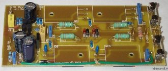
PRINTED BOARDS FOR HOLTON AMPLIFIER
Below are collected drawings of printed circuit boards for the Holton amplifier, posted on the “SOLDERING IRON” and “A BIT OF AUDIO EQUIPMENT” forums, and of course my own options. All files are packed in WINRAR and in LAY 5 format; click the picture you like to download. Opens the gallery of printed circuit boards with a drawing with two pairs of terminal transistors. In this version, the radiators for transistors are separate, the board has dimensions of 80 x 90 mm:
Another version of a printed circuit board with two pairs in the final stage, but no longer IRFP240 - IRFP9240, but IRF640 - IRF9640. The board is made for SMD components and has two channels at once. Board size 158 x 73 mm:
The next option closely resembles the classic arrangement of parts as in the original Holton amplifier. The board is designed for installing two pairs in a window cascade and a common radiator for UNA transistors. Size 124 x 89 mm:
Another option with two output pairs, size 111 x 39 mm, ALL UNA transistors on one radiator:
The next option uses 4 pairs of terminal transistors and is capable of delivering up to 400 W to the load. Board size 182 x 100 mm:
A monster with ten pairs and an installed compensator has a size of 280 x 120 mm, most likely for a load of 2 Ohms:
A universal board for the Holton amplifier, which allows you to increase the number of pairs of transistors in the final stage. The drawing is multi-page, the board is two-tiered, the appearance of the 200 W amplifier is shown below, transistors 2SD669A and 2SB649A are installed:
Due to IR's refusal to produce IRFP240 - IRFP9240, the quality of the transistors noticeably deteriorated, so it was decided to rework the Holton amplifier into a universal output stage using 2SA1943 - 2SC5200 transistors, which also has overload protection. The result is the following design:
This board also has the ability to expand output transistors, and on the voltage amplifier board it is possible to connect a separate power source, only for UNA:
More details about this circuitry are written HERE. Or you can watch the video:
All that remains is to make the board, solder the parts and before turning it on, read the information below.
ADJUSTING THE HOLTON AMPLIFIER
Before you begin setting up Eric Holton's power amplifier, you should take a closer look at the circuit. On the page with the description of the scheme, some explanations were already given and several diagrams were given. On this page we will look at another circuit of the same amplifier, but already made in a simulator, which will allow you to check many parameters, rigorously experiment with the elements, identifying the consequences of errors during installation and the use of low-quality element base. So, the experimental circuit of the Holton amplifier looks like this:
This circuit contains only two pairs of final transistors only for experiments in the simulator and a more compact display on the page. In reality, the number of final transistors directly depends on the required output power, regardless of the load resistance - one pair of transistors IRFP240 - IRFP9240 can safely deliver about 100 W to the load, therefore, to obtain 200 W you will need two pairs, and to obtain 800 W you already need 8 steam in the final stage. For those who are not very comfortable with a calculator, here is a table of the dependence of the output power on the supply voltage and the required number of pairs of transistors in the final stage:
| PARAMETER | PER LOAD | ||
| 8 ohm | 4 Ohm | 2 Ohm (4 Ohm bridge) | |
| Maximum supply voltage, ± V | ±85 V | ±85 V | ±60 V |
| Maximum output power, W at distortion up to 1% and supply voltage: | The required number of pairs of terminal transistors is indicated in parentheses. | ||
| ±30 V | 40 W (1) | 80 W ( 1 ) | 160 W (2) |
| ±35 V | 60 W (1) | 120 W ( 1 ) | 240 W (3) |
| ±40 V | 80 W ( 1 ) | 160 W (2) | 320 W (4) |
| ±45 V | 100 W ( 1 ) | 200 W (2) | 400 W (5) |
| ±50 V | 135 W (2) | 270 W (3) | 540 W (6) |
| ±55 V | 160 W (2) | 320 W (4) | 640 W (7) |
| ±60 V | 200 W (2) | 400 W (4) | 800 W (8) |
| ±65 V | 240 W (3) | 480 W (5) | DO NOT TURN ON!!! |
Depending on the supply voltage, the voltages at the control points also change. The voltage map below will allow you to navigate not only the operating modes, but also in troubleshooting the Holton amplifier:
| VOLTAGE MAPS | ||
| SUPPLY VOLTAGE | VOLTAGE | CURRENT |
| ±40 V | ||
| ±50 V | ||
| ±60 V | ||
| ±70 V | ||
| ±80 V | ||
| ±90 V | ||
First of all, you should pay attention to the value of resistors R3, R7 and R8. It is these resistors that set the current operating modes of the first stages, which directly affect the operation of all subsequent ones. It's no secret that with the same resistance and different voltages, the current through the resistance will change. Actually, this explains the difference in resistance ratings R3, R7 and R8. Of course, the ratings given in the original circuit will maintain the functionality of the amplifier over the entire range of supply voltages, but changing them will significantly reduce the THD level. Namely, this parameter is often the main one when choosing a scheme. In addition, changing the ratings also changes the power dissipation of transistors Q3 and Q4, reducing their self-heating and improving the thermal stability of the amplifier. If you are making an amplifier for yourself, and not for drinking, then it makes sense to pay attention to this factor. Even with changed resistors, the upper transistors heat up: Self-heating does not have much effect on the operating modes of the cascades - the current generator on transistor Q2 keeps the current in a given range and the current of the following cascades remains almost unchanged. Nevertheless, if it is possible to reduce the heating, then why not do it? Essentially, the differential stage is used to obtain high-quality negative feedback and does not introduce amplification into the input signal. Transistors Q3 and Q4 also do not amplify the voltage - they form a bias for the next stage. The main increase in the amplitude of the input signal occurs at transistor Q11. The THD level is also influenced by its own gain, so when building an amplifier with an output power above 500 W, the question may arise of using a pre-amplifier or introducing a buffer op-amp into the amplifier. For example, let's take our own gain equal to 36 dB. To obtain a voltage amplitude of 63 V at the output of the amplifier, we need to apply 1 volt to the input. The THD level in this case will be more than 0.07%:
With a native gain of 30 dB and an output voltage of 63 V, the THD level decreased by almost 2 times, although 2 V was already required to be supplied to the input:
The gain factor depends on the ratio of the values of resistors R14 and R11 and can be approximately calculated using the formula Kу = (R14 / R11) + 1.
The figure below shows the shape and magnitude of the voltages in the circuit:
Blue line - voltage at base Q1
;
Red - voltage at collector Q3
;
Green - voltage at collector Q11
.
The conclusion from this is not difficult to draw - transistor Q11 must have the highest possible gain, and since Q6 works with it in a differential stage, its gain must be equal to the gain of Q11. The magnitude of the gain of the transistor directly determines what current is required to open it, i.e. how heavily the previous cascade will be loaded, the load of which also determines the THD level - the less the current changes
, the less THD will be. To select transistors, you can, of course, use the socket available on most digital multimeters, but the actual gain koff parameter on this socket can only be obtained for low-power transistors. For medium and high power transistors, you can only choose the same ones with maximum parameters. You can read about the reasons for such disgrace HERE or look HERE. Concluding the resistive saga of the voltage amplifier, it is worth mentioning resistors R4 and R9. As already written on the page describing the circuit, the values of these resistors quite strongly influence the THD level. For example, let's take the value of these resistors equal to 100 Ohms, as in the original circuit, and calculate the THD level:
Well, in principle, the THD level of 0.065% is even less than the 0.08% declared on most sites, but we won’t be lazy when buying parts and choose 2N5551 transistors with the highest possible and SAME gain factor. This will give a reason to reduce R4 and R9 to 22 Ohms and we will get the following THD level:
The scale of the grid was preserved intentionally to give you a feel for what happens when you change two values, but after preliminary rejection of the element base - THD dropped to a value of 0.023% and this is with an output amplitude of 63 V and a gain of 30 dB. Now all that remains is to play around with the resistor values of the final stage, namely with the resistors installed on the gates of the final transistors. 100 Ohm... From one side it doesn’t seem like much, but taking into account that the gate capacitance is 1200-1300 pF, it makes sense to think about it and model something like this:
In this circuit, the voltage amplifier is excluded, and instead two square-wave generators V1 and V2 are used, operating in antiphase. Thus, V1 controls the positive arm of the final stage, and V2 controls the negative arm. The constant voltage source V3 provides the quiescent current of the final stage. We can check the parameters of ONLY the final stage and we will see what is happening at the output of the “amplifier” and at its input if there are 100 Ohm resistors in the gate circuits:
The blue line is the voltage at the right pin of R1, i.e. voltage coming from the UNA. The red line indicates the voltage supplied to the load. You don't need to have good eyesight to see the surges and collapse of fronts and rectangular recessions. If anyone hasn’t counted, then this is a frequency of 16 kHz. Now let’s halve the value of the resistors in the gates and get the following:
It is not difficult to guess what shape the rectangle will take when using 470 Ohm resistors installed in the original amplifier, so I will not attach a drawing. Why are 100 ohm resistors used and not smaller? Well, let's try to figure it out... First of all, the IRFP240 - IRFP9240 transistors were not developed for AF power amplifiers and such a parameter as gain is not standardized for them. However, to select the same transistors, while they were produced by International Rectifier
(IR) was not at all difficult - one or two, or even more than one transistors were rejected from one standard package, but
something was wrong Vishay Siliconix
You can, of course, turn to “sound” field workers, but their price is quite high, so let’s return to the resistors in the gates and see what current the voltage supply actually gives to recharge these same gates. To do this, let’s take a model of a full-fledged amplifier with eight pairs of terminals, and as a measuring tool we’ll take the voltage drop across additional resistors R19 and R20 (highlighted in green):
At a frequency of 16 kHz and an output voltage of 63 V, the drop across a resistance of 1 Ohm was 0.025 V, which corresponds to a current flowing through the resistor of 0.025 A (green background). With an output power close to clipping (see bottom of page), the drop across the same resistor is already 0.033 V, i.e. 0.033 A is required to recharge eight pairs of gates in the final stage. Considering that the original Holton amplifier uses KSE340 - KSE350 transistors with a maximum current of 0.5 A, it becomes clear why the resistors must be at least 100 Ohms. However, above there is a table of possible replacements and there ALL transistors have a collector current of at least 1 A, which allows you to abandon the so-called gate capacitance compensator proposed by Holton, and connect the gates directly to the output of the voltage amplifier. The values of the gate resistors can also be reduced if fewer pairs of end-of-line transistors are used. The rating can be calculated by proportion based on the fact that for eight pairs 100 Ohms are needed, and for 4 pairs 50 Ohms will be quite enough, even when used in the KSE340 - KSE350 amplifier. Below 15 Ohms, it is better not to use resistors in the gates of terminals - in addition to limiting the recharge current, they also compensate for the spread of parameters a little.
So, we’ve sorted out the ratings, installed and soldered all the elements of the circuit, according to our concepts, we can start turning them on for the first time. However, before this, it is necessary to exclude the final transistors from the circuit, and instead of them, temporarily solder permanent resistors with a power of 0.5 - 1 W and a resistance of 10 - 15 Ohms. This measure is dictated by the cost of the terminal transistors - if all the elements are in place and they are in good working order, and there are no unplanned jumpers on the board resulting from inaccurate soldering, then in this option the functionality of the voltage amplifier will simply be checked. If there are snot on the board, elements are misplaced, or they are not working properly due to overheating during installation or were initially defective, then the power part that can fail will remain intact. Ultimately, the Holton amplifier circuit for the first turn on looks like this, where R31 and R32 imitate the final stage and close the OOS circuit to bring the voltage amplifier into operating mode:
The voltages on the actual board should not differ by more than 2% from the voltages shown on the maps. By the way, in the proposed version of the amplifier circuit there are no resistors connected in series with diodes D4 and D7. This was done to obtain at least a small, but still increase in output power. These resistors are not of particular importance during operation of the amplifier, but by the amount of smoke from them, in the event of installation errors, you can determine the degree of error. Therefore, it is strongly recommended, in order to save budget, to include resistors with a resistance of 10-15 Ohms in series with diodes D4 and D7. After checking their functionality, they can be removed. Before switching on for the first time, the tuning resistor R16, both on the model and on the real circuit, MUST be set to the MAXIMUM resistance position. On a real diagram. In this case, the quiescent current of the terminal transistors is the minimum possible. Now let's get back to the actual circuit:
Assemblies C1-C3 and C7-C9 are analogues of a high-capacity non-polar capacitor; it is better to use electrolytes of the WL or WZ series, the so-called computer ones, with silver or gold markings. If possible, it is better to double the electrolyte ratings - the frequency response in the low-frequency region is smoother, although even in this level it remains within 1.5 dB. Capacitors C14, C15, C16 and C17 in the circuit are 47 pF. These ratings were used to increase stability, although with its own gain of up to 27 dB, the amplifier is quite stable even when installing 22 pF capacitors. After checking the functionality of the voltage amplifier, the final stage is mounted on the board, installed on the radiator and the quiescent current is adjusted. With the final cascade of the first, it is better to switch on either through current-limiting resistors installed in each power arm, or turn on an incandescent lamp with a power of 40-60 W in series with the primary winding of the transformer. If the voltages at the control points correspond to the calculated ones, then the current-limiting circuits are eliminated, of course, turning off the power supply and allowing the power filter capacitors to discharge, and then the quiescent current is regulated. Quite often, a quiescent current of 100 mA is recommended for a Holton amplifier, but it was not possible to detect any difference in sound quality with a quiescent current from 45 mA to 150 mA, so it is better to use the golden mean - a quiescent current in the range of 50-60 mA, especially The simulator shows that at this quiescent current there is a minimum THD level. Well, that’s actually the whole amplifier, at the end of the day an earlier version of the recommendations for assembling the two-story version.
A FEW WORDS ABOUT HOW TO CORRECTLY ASSEMBLE AN AMPLIFIER A variant of the description of an old article.
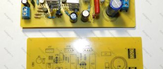
For example, consider a module with two pairs of terminal transistors, as the most popular. The assembly technology of the remaining options differs only in the amount of fasteners used. To install the amplifier, you need to check whether the legs of the resistors “marked” with a marker are broken (item 1) and unsolder the jumper legs connecting the “back” part of the structure (item 2, Fig. 3).
Figure 3.
By the way, the appearance of the pre-amp board for the O-7 and O-8 sets has a slightly different appearance, since higher voltage transistors are used (Fig. 4).
Figure 4.
After desoldering, the upper board should be bent and the lower board should be screwed to the radiator using M-3 screws. Mica spacers must be placed under the output stage transistors and the quiescent current stabilization transistor. You should also install a heat sink on the transistors of the current sources and the penultimate stages on the pre-amplifier board (positions 1 and 2 in Fig. 5). The dimensions between the holes on the preliminary stage board are selected in such a way that half of the S-370 processor radiator fits there perfectly, in which you only need to drill 2.5 mm holes and cut an M-3 thread. If you don’t have anything similar at hand and have nowhere to get it, then you can use a piece of aluminum corner (item 1 in Fig. 6 there is a corner from an aluminum cornice on which curtains are hung) or a channel bar.
Figure 5. Figure 6.
Then the upper board is bent into its original position and the jumper legs 2 are soldered (Fig. 6) and once again it is checked whether the terminals of resistors 3 are bitten. Perhaps it is worth explaining what kind of resistors these are... When soldering the bitten part of these resistors, the preliminary stage board can be turned on without a terminal cascade, which is very convenient when setting up and repairing an amplifier. That is, power is supplied directly to the pre-amplifier board and in the event of a malfunction on the pre-amplifier board, the final transistors are not in danger. After installing the heat sinks, you should apply the supply voltage and set the quiescent current of the final stage using a trimming resistor. To do this, measure the voltage across the current-limiting resistors of 0.22 Ohm and by rotating the slider, achieve a millivoltmeter reading of 0.022 V, which will correspond to a current of 100 mA (of course, the input to ground). At this point, the adjustment can be considered complete and all you have to do is enjoy the pleasant sound of this amplifier. The amplifier gain can be calculated using the formula R21+1/R6. The resulting result shows how many times the input signal will be amplified. To obtain the gain factor in dB, you must use the formula Kdb = 20 x log Kr, where Klb is the gain factor in dB, Kr is the gain factor in times, lg is the decimal logarithm, 20 is the multiplier. For an example, the equality of the gain in times and dB is given in the table. It is not recommended to make the power amplifier gain more than 30 dB, as this leads to an additional increase in THD and the tendency of the amplifier to excite.
| GAIN KOF | ||||
| ONCE | dB | ONCE | dB | |
| 2 | 6 | 15 | 23,5 | |
| 3 | 9,5 | 20 | 26 | |
| 4 | 12 | 25 | 27,9 | |
| 5 | 13,9 | 30 | 29,5 | |
| 6 | 15,5 | 35 | 30,8 | |
| 7 | 16,9 | 40 | 32 | |
| 8 | 18 | 45 | 33 | |
| 9 | 19 | 50 | 33,9 | |
| 10 | 20 | 55 | 34,8 | |
And finally, we cannot keep silent about some additional advantages of the final stage boards - all high-current tracks are reinforced, for sets O-1...O-3 with a single-core winding wire with a diameter of 0.7 mm, for sets O-4...O-6 with acoustic wire cross-section 0.75 mm kV, for connections O-7 and O-8 with acoustic cable cores with a cross-section of 1.5 mm kV (Fig. 7, O-8 module board without end-of-line transistors).
Figure 7.
Figure 8 shows the connection diagram for the O-2 module; the connection for other modules is similar.
Clipping on the oscilloscope screen.
Instead of a pure harmonic wave, the sine wave is cut off at the top and bottom - the tops are flat instead of rounded.
You can see more details about how much power a power supply is needed for a power amplifier in the video below.
The STONECOLD amplifier is taken as an example, but this measurement makes it clear that the power of the network transformer may be less than the power of the amplifier by about 30%. Site administration address
Using auxiliary programs
You can achieve the purest audio playback by using a do-it-yourself audio amplifier in your car. But for this purpose you will need to create a circuit yourself using auxiliary programs/tools.
For example, Sprint Layout is used for designing circuits of varying complexity, wiring, visualization of three-dimensional models, and compiling a library of elements.
The program will allow you to make a visual plan, which will be more useful than photographs of a homemade amplifier for a car, made by yourself, and its parts.