Specifications
First of all, the capabilities of the transistor depend on the maximum permissible characteristics. Exceeding them during operation will result in device failure. For KT837 they are equal:
- constant voltage K-B: KT837A, B, V, L, M, N, 2T837A, G – 80 A;
- KT837G, D, E, P, R, S, 2T837B, D – 60 V;
- KT837ZH, I, K, T, U, F, 2T837V, E – 45 V;
- KT837A, B, V, L, M, N, 2T837A, G – 70 A;
- KT837A, B, V, L, M, N – 60 A;
- KT837A-K, 2T837A-V – 15 V;
- KT837A-F – 7.5 A;
- without heat sink – 1 W;
In addition to the maximum, the capabilities and scope of application of the KT837 are also affected by the electrical characteristics. They were measured at a temperature of +25°C. Other testing parameters that can affect the final result are listed in the following table in a separate column.
| Electrical characteristics of the KT837 transistor (at T = +25 o C) | |||||
| Options | Test Modes | Tr-r | min | max | Unit change |
| Static gain in the OE circuit | UKB = 5 V, IE = 2 mA | KT837A, L, G, P, F, T | 10 | 40 | |
| KT837B, M, D, R, I, U | 20 | 80 | |||
| KT837V, N, E, S, K, F | 50 | 150 | |||
| Reverse current K-E | UKE = UKE max | ALL | 10 | mA | |
| Reverse current K-B | UKb = UKb max | ALL | 0,15 | mA | |
| Reverse current through E | UEB = 15 V | KT837A-G | 0,3 | µA | |
| UEB = 5 V | KT837L-F | 0,3 | |||
| Saturation voltage K-E | Ik= 3 A, Ib= 0.37 A | KT837A-V, L-N | 2,5 | IN | |
| Ik= 3 A, Ib= 0.37 A | KT837G-E, P-S | 0,9 | |||
| Ik= 2 A, Ib= 0.3 A | KT837Zh-K, T-F | 0,5 | |||
| Saturation voltage B-E | Ik= 2 A, Ib= 0.5 A | ALL | 1,5 | IN | |
Universal sound amplifier
An interesting circuit design is discussed on the radio chip website for a simple universal audio amplifier.
The website offers a version of a universal amplifier cell (Figure 1), convenient for manufacturing it in the form of a microassembly or microcircuit. Its use will significantly simplify many radio equipment components that require signal amplification and low-impedance loads, and will also allow you to eliminate the need for a printed circuit board by placing the chip on a radiator.
If you install a symmetrical repeater using bipolar transistors at the input of a universal audio amplifier with a dynamic load, you can perfectly match the input and output characteristics of the transistors. Since the base currents of the input transistors are equal and mutually opposite, all modes of subsequent transistors are set automatically (on mutual compensation).
According to the circuit in Fig. 2, two amplifiers are assembled using germanium and silicon transistors (1 W and 10 W). Their gain when operating with a load of 10 ohms is 75 and without a load 800, 1200 (R = 1 kOhm, R8 = 1 kOhm). The output signal level does not depend on changes in supply voltage, so the audio amplifier does not require stabilized power supplies (with bipolar power supply). The input impedance of the amplifier is 25 kOhm with a load resistance of R7 = 10 Ohm and increases as it increases to 50 kOhm.
Capacitors C2 and SZ are necessary to eliminate possible self-excitation of the amplifier in voltage amplification mode. Their capacity is 1000 – 1500 pF. When working with a bipolar power supply, you can eliminate the input capacitor C1 and resistors R1, R2.
In this case, resistors R3, R4 need to eliminate the DC component at the amplifier output relative to the zero point of the power source. The frequency response of the amplifier is linear up to 20 kHz and has a slight decline (20%) at 30 kHz (with capacitors C2, C3).
To eliminate step-type distortion at low signal levels, resistors R3 and R4 should be used to set the current of the output transistors to 10 ... ... 12 mA. If there are no special requirements for the amplifiers, then transistors need not be selected, but their maximum permissible voltage should be higher than the supply voltage.
The gain can be adjusted by changing the feedback value Roс (R8). At maximum feedback, the gain is 1. The amplifier is an ideal signal follower with maximum nonlinear distortion. (All measurements were carried out with an oscilloscope). The amplifier circuit (Fig. 2) is designed for one power source (the amplifier gain is 1 if points 3 and 4 are short-circuited (Fig. 1), and the gain is maximum if point A is grounded and connected to power supply 0).
Due to the absence of deep negative connections, the amplifier does not produce phase distortions, and nonlinear distortions are minimized by selecting pairs of transistors with identical parameters. Transistors VT1 and VT3 can be replaced with KT3102, KT503, VT2, VI4 - with KT3107 and KT502, respectively. VT7 - on KT835 - KT837, VTS - but KT305 with any letter index.
All transistors are selected according to the permissible supply voltage in complementary pairs. Option of a 1 W amplifier on germanium transistors: VT1, VT3, VT6 type MP35-MP38; VT2, VT4, VT5 type MP39-MP42; VT7 type PG402 (GT703); VT8 type GT404 (GT705). Resistors R3, R4 increase to 25 - 30 kOhm. Supply voltage ±5 V (10 V for unipolar). The load resistance in both amplifiers can vary from A to 10 Ohms. It is necessary to provide heat removal from transistors VT and VT8 (with a corresponding radiator).
Analogs
To replace the KT837, the following foreign analogues can be offered:
| KT837 series transistor | Foreign analogue |
| KT837A | TIP42C |
| KT837B | BD302 (you can also use the domestic KT818B) |
| KT837V | 2SB834 (KT835B can be used) |
| KT837G | BD244A |
| KT837D | 2N6111 |
| KT837S | BD225 |
| KT837K | TIP127 (domestic KT8115A is also suitable) |
| KT837E | BD277 |
| KT837F | BD224 |
| KT837H | BD223, 2N6107 |
| KT837X | NTE197 |
For KT837 transistors, a complementary pair is provided - KT805.
Connection schemes
Using the KT837 you can build a simple audio amplifier with the following parameters:
- Power – 30 W / 4 Ohm (15 W / 8 Ohm);
- Harmonic content – 0.01%;
- Input impedance – 47 kOhm;
- Output impedance – 0.03 Ohm;
- Noise level – -86 dB.
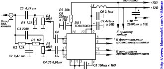
This amplifier uses ceramic capacitors rated at 50 V. There are two options for mounting the board.
Firstly, on the heat sink of transistors VT5 and VT6, using racks with a height of 15 to 20 mm.
Secondly, next to the heat sink of the final stage. In this case, the MRN-22 connector is used for connection, which will provide contact at the points indicated on the diagram by numbers from 1 to 5. To prevent the transistor from burning out, if contact is lost in the plug, it is necessary to increase the resistance of resistors R12 and R13 to 43-47 Ohms , and on the other side of the socket install R121 and R131 (drawn in dashed lines in the diagram) of the same rating (43-47 Ohms). The length of the wires connecting the board and transistors should not be more than 10 cm.
Instead of the specified operational amplifier, you can install K140UD6B, K140UD7A, K544UD1A, but the harmonic content will increase to 0.3%.
Transistors VT3 and VT4 are installed on a heat sink made of an aluminum plate measuring 70x35x3 mm.
There are two ways to secure VT5 and VT6.
The first method is on a heat sink common to each amplifier channel. Transistor VT5 is attached in the same place as VT3, and VT6 together with VT4. In this case, the heat sink must be isolated from the ULF housing. In this case, you can use transistors in a plastic case.
The second method is on a heat sink common to both transistors of the final stage. In this case, you need to insulate the transistor with mica spacers and use thermal paste to improve heat transfer. In this case, it is recommended to install the devices in a metal casing.
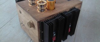
In any case, the heat sink area per transistor must be more than 500 square centimeters.
Simple high quality Gumel amplifier (42 W/4 Ohm)
Analysis of letters from radio amateurs allowed us to come to the following conclusions. Firstly (and this is natural), everyone is in favor of creating simple circuitry AF power amplifiers (UMZCH); secondly, the simpler the amplifier circuit, the less trained radio amateurs undertake its assembly; thirdly, even experienced designers often ignore known installation rules, which leads to failures when repeating UMZCH on a modern element base.
Based on the above, the UMZCH was developed (see Fig. 1). Its main features are the use of op-amps in small-signal mode, which expands the frequency band of signals reproduced without exceeding the slew rate of the op-amp's output voltage; transistors of the output stage - in the OE circuit, and the pre-final stage - with a divided load in the emitter and collector circuits. The latter, in addition to the obvious design advantage - the possibility of placing all four transistors on a common heat sink, provides certain advantages compared to the output stage in which the transistors are connected according to the OK circuit.
Main technical characteristics of UMZCH:
Nominal frequency range with frequency response unevenness 2 dB: 20 – 20000 Hz
Rated output power: 30W/4ohm (15W/8ohm)
Maximum output power: 42 W/4 ohms (21 W/8 ohms)
Harmonic distortion at rated power in rated frequency range: 0.01%
Nominal (maximum) input voltage: 0.8 (1) V
Input impedance: 47 kOhm
Output impedance: no more than 0.03 Ohm
Relative noise and background level: -86 dB
Amplitude of output voltage surges when turning the UMZCH on and off: 0.1 V
Description
Op-amp DA1 is powered through transistors VT1 and VT2, which reduce the supply voltage to the required values. The quiescent currents of the transistors create voltage drops across resistors R8 and R9, sufficient to provide the required bias voltage at the bases of transistors VT3, VT4 and VT5, VT6. In this case, the bias voltages for the transistors of the final stage are chosen such (0.35-0.4 V) that they remain reliably closed when the supply voltage increases by 10-15% and overheats by 60-80 °C. They are removed from resistors R12, R13, which simultaneously stabilize the operating mode of the transistors of the pre-final stage and create local negative feedback on current.
The relationship between the resistances of resistors R11 and R4 of the OOS circuit is selected from the condition of obtaining a nominal input voltage of 0.8 V. The inclusion of external correction and op-amp balancing circuits is not shown in the diagram for simplicity (this will be discussed in the section devoted to setting up the amplifier).
Low-pass filter R3C2 and high-pass filter C3R10 with cutoff frequencies in the region of 60 kHz prevent the operation of relatively low-frequency transistors VT3-VT6 at higher frequencies in order to avoid their breakdown. Capacitors C4, C5 correct the phase response characteristics of the pre-terminal and final cascades, preventing their self-excitation if installation is unsuccessful.
Coil L1 increases the stability of the UMZCH with a significant capacitive load.
The UMZCH is powered by an unstabilized rectifier. It can be common to both channels of the stereo amplifier, but in this case the capacitance of filter capacitors C8 and C9 must be doubled, and the diameter of the wire of the secondary winding of transformer T1 must be doubled. Fuses are included in the power supply circuit of each amplifier.
The design of the UMZCH can be different, but some design features on which the success of its repetition depends must be taken into account.
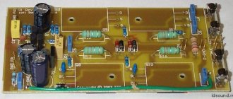
Printed circuit board of one amplifier channel:
The length of the leads of the parts should be no more than 7-10 mm (for ease of installation, the leads of the op-amp DA1 are shortened to approximately 15 mm). In UMZCH it is necessary to use ceramic capacitors with a rated voltage of at least 50 V. The board can be mounted on the heat sink of the transistors of the final stage using racks 15-20 mm high or in close proximity to it, using any detachable connector to connect the final stage to the pre-terminal stage, for example MRN-22 (sockets and connector pins are connected at points 1-5). In the latter case, the resistance of resistors R12 and R13 should be selected equal to 43-47 Ohms, and on the connector socket with transistors VT5, VT6 connected to it, resistors of the same resistance R12′ and R13′ should be installed (this will prevent failure of the transistors if contact is lost in the connector ). The length of the conductors between the board and the transistors of the final stage should be no more than 100 mm.
In addition to what is indicated in the diagram, the UMZCH can use op amps K140UD6B, K140UD7A, K544UD1A, however, the harmonic coefficient at frequencies above 5 kHz will increase in this case to approximately 0.3%.
The transistors of the pre-terminal stage are placed on a heat sink, bent from a plate with dimensions of 70x35x3 mm (excluding a tab with a hole with a diameter of 2.2 mm) made of aluminum alloy, which is attached to the board with one M2x8 screw and nut to prevent breakage of the transistor leads due to accidental mechanical impacts.
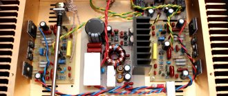
The transistors of the final stage can be placed either on a heat sink common to each channel of the UMZCH, or on a heat sink common to both channels. In the first case, they are fixed to the heat sink and the latter is isolated from the UMZCH case; in the second case, the transistors are isolated, and the heat sink can be a structural element of the amplifier case. To reduce the thermal resistance of the transistor body - heat sink, it is necessary to use thermal conductive paste. When using separate (for each channel) heat sinks, you can use transistors in a plastic case, which, due to the small area of the metal bases, can overheat if the gaskets are poorly made or the thermal contact with the heat sink is loose and there is an excessive amount of paste in the gap. It is advisable to install transistors in a metal case on a heat sink common to both channels. The heat sink area per transistor must be at least 500 cm2.
The installation of the UMZCH and the connection of its channels to the power source are of great importance. The power wires (+22 V, -22 V and common) should be as short as possible (they should be laid separately for each channel) and of a sufficiently large cross-section (with a maximum power of 42 W - at least 1.5 mm2). Wires of the same cross-section must be used to connect the speaker systems, as well as the emitter and collector circuits of the final stage transistors to the UMZCH board.
They set up the UMZCH with the final stage turned off. If a detachable connector is used to connect parts of the UMZCH, it is convenient to use a technological socket to which only the power wires and the output of the AF signal generator are connected. When directly connecting the terminal transistors to the UMZCH board, it is enough to remove the solder jumpers from the printed conductors of their base circuits and temporarily solder the latter to the emitter terminals.
To balance op-amp DA1 (if the need arises), the board has holes for trimmer and fixed resistors or wire jumpers to connect the pins of the microcircuit in accordance with the balancing circuit for a specific type. For example, to balance the K544UD2 op-amp, its terminals 1 and 8 are connected through a resistor with a resistance of 62 kOhm to the output of the engine and one of the terminals of the resistive element of a trimmer resistor with a resistance of 22 kOhm. The free pin of this resistor is connected by a wire jumper to pin 7 of the op-amp, and through a resistor with a resistance of 75 kOhm to pin 5 (in Fig. 2 these elements are shown with dashed lines). When using the K544UD1 op-amp, its pin 1 is connected through a resistor with a resistance of 4.3 kOhm to the terminals of a trimming resistor with a resistance of 1.5 kOhm. Its free pin is connected to pin 8 of the op-amp through a resistor with a resistance of 5.1 kOhm, and to pin 7 with a jumper wire. To balance the op-amps K140UD6 and K140UD7, resistors of the same values are used, but the free output of the adjusted resistor is connected through a constant resistor to pin 5, and by a jumper to pin 4 of the op-amp. However, balancing may not be necessary, so these parts are installed only if necessary.
The setup begins with the input of the amplifier being short-circuited, an oscilloscope turned on in maximum sensitivity mode is connected to the output, and power is applied briefly. If there is no AC voltage at the output, i.e. there is no self-excitation; the operating mode of transistors VT3, VT4 and op-amp DA1 is measured using direct current. The op-amp supply voltages should be within the range of +13.5...14 and -13.5...14 V and be approximately the same (deviation is acceptable within 0.2-0.3 V). The voltage drop across resistors R12 and R13 should be equal to 0.35-0.4 V. If they differ significantly (by more than 10%) from the specified value, it is necessary to select resistors R8, R9, making sure that their new resistance remained the same. Replace resistors when the UMZCH power is turned off. The approximate resistance of resistors for the K544UD2A op-amp is indicated in the diagram. When using op-amps K544UD1A and K140UD6, their initial resistance should be 680 Ohms, and when using K140UD7 - 560 Ohms.
Having selected resistors R8, R9, measure the DC voltage at the output of the UMZCH and, if it exceeds 20-30 mV, balance the op-amp DA1. Then connect the bases of transistors VT5, VT6 to the emitters VT3, VT4 and, briefly turning on the power, make sure that even in this form the UMZCH does not self-excite. The AC noise and background voltage when the input is short-circuited should not exceed 1 mV.
Next, a resistor with a resistance of 16 Ohms with a dissipation power of 10-15 W is connected to the output of the UMZCH, the input of the UMZCH is opened, a generator tuned to a frequency of 1 kHz is connected to it and, gradually increasing its signal until a voltage of 13.5-14 V is obtained at the load, the symmetry is checked limitations of positive and negative half-waves of a sine wave.
The minimum (within the specified limits) constant voltage at the output of the amplifier is achieved, if necessary, by final balancing of op-amp DA1. After this, you can begin to measure the main characteristics of the UMZCH by loading it with a nominal load - a resistor with a resistance of 4 or 8 Ohms.
It should, however, be taken into account that an attempt to adjust, and even more accurately evaluate the parameters of a UMZCH assembled without observing the above installation rules, without installing it in the place intended for it and without powering it from its own power supply, will not only not give the desired result, but it can also lead to failure of the output stage transistors. Setting up the UMZCH and measuring its characteristics should be started only after its design has been completely completed. The simplicity of the amplifier is only apparent. We should not forget that both the DA1 op-amp and the UMZCH as a whole use transistors with maximum generation frequencies of 100-300 MHz, and in the output stages - with significant transition capacitances, which can lead to self-excitation even in the apparent absence of feedback circuits and loads of sufficient magnitude. The insignificant inductance of the emitter circuit wire, the parallel arrangement of the base and collector circuit wires over a significant length can cause self-excitation at high frequencies, which is extremely dangerous for transistors of the final and pre-terminal stages. (However, this is true not only for the device described, but also for UMZCH assembled according to any other scheme.)
When measuring the harmonic coefficient and the relative level of noise and interference, you should remember about possible interference from the power supply network, television and radio transmitters, televisions and other radio devices due to poor shielding of connecting wires, the UMZCH input and sensitive measuring instruments, as well as in the absence of their connection ungrounded enclosures to each other. Sometimes it is enough to rearrange the power plug of one of the devices or UMZCH in the socket to get the wrong result. By the way, you should not use the method of checking the UMZCH, known from old amateur radio practice, by touching its input circuit with your finger. This can lead to such a level of high-frequency interference that the output transistors fail.
The considered circuit can be taken as a basis when creating UMZCH with different output powers. To do this, you just need to change a number of elements of the UMZCH and the power supply. Some recommendations on this matter can be gleaned from the table. When constructing a UMZCH with an output power of approximately 25 W, some elements can be eliminated (see Fig. 3). As you can see, instead of a resistor in the circuit of the non-inverting input of op-amp DA1, connected to a common wire, a divider of resistors R1-R3 is used here, which made it possible to abandon the middle terminal of the secondary winding of the network transformer T1. This allows the use of transformers with a secondary winding voltage of 24-28 V and protects the speaker system from failure if one of the final stage transistors breaks down.
UMZCH according to the diagram in Fig. 3 can be mounted on the same PCB (see Fig. 2). In this case, the holes for the terminals of resistors R2, R5-R7 are left free, resistors R8 and R9 are soldered directly into the power circuit of the op-amp DA1, for which wire jumpers are installed in the holes for the terminals of the emitters and collectors of transistors VT1, VT2. With an output power of less than 25 W, transistors of the KT805 and KT837 series with any letter indices can be used in the final stage.
Note. The resistances of resistors R8, R9 (UMZCH according to the diagram in Fig. 1) and R6, R7 (UMZCH according to the diagram in Fig. 3) are indicated approximately. Setting up UMZCH according to the diagram in Fig. 3 is no different from the one described above.
Author: Gumelya E.