Project 101 – FET amplifier from Rod Elliott
I have often said that I am not a fan of FET power amplifiers, but this amplifier has changed my views and I consider it a "benchmark" system in every way. It uses field effect transistors. Performance is very good, with incredibly low distortion, high power, wide bandwidth and "self-protecting" output transistors. But this does not mean that the amplifier will not fail, it is just that it is much more tolerant of failures than a bipolar transistor amplifier, and only a pair of zener diodes are required to limit the current.
All traces on the printed circuit board are made as short as possible, which minimizes the likelihood of noise. The amplifier will operate stably at supply voltages from ±5 V to ±70 V.
With a supply voltage of ±70 V (which must not be exceeded!), the output power is approximately 180 W/8 ohms or 250 W/4 ohms. Short-term power about 240 W/8 Ohm or 380 W/4 Ohm. The recommended supply voltage is ±56 V.
If maximum power is not needed, I suggest using a ±56V supply voltage obtained from a transformer with 40V + 40V secondary windings. You will get about 150W/8ohms of power from this voltage, and also reduce the requirements for the output transistors and radiators.
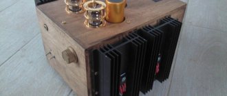
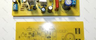
The photo shows the printed circuit board. The output transistors are mounted under the board and secured with screws. No other installation is required. The green conductor along the leading edge of the board is ground, so that the main current-carrying traces are not damaged. The entire input part is located between electrolytic capacitors and is intentionally as compact as possible. This improves performance by ensuring there are no long traces for the input stage that could otherwise pick up noise that could seriously degrade the sound.
Characteristics:
| output power | > 180 W | <1% THD, 8 ohms |
| > 275 W | <1% THD, 4 ohms | |
| DC offset | <20 mV | typical |
| Noise | RMS <2 mV | Unweighted (-54 dbV) |
| THD | 0,015% | No load, voltage 30 V, 1 kHz |
| 0,017% | 8 Ohm, voltage 30 V, 1 kHz | |
| 0,02% | 4 Ohm, voltage 30 V, 1 kHz | |
| Output impedance | <10 mOhm | 1 kHz, 4 ohm load |
| <25 mOhm | 10 kHz, 4 ohm load | |
| Frequency range | 10 – 50000 Hz | At 1 W -1.5 dB |
The distortion values show that the load on the amplifier produces very little deviation. There are no visible or audible high-order components in the distortion form. Output impedance was measured on a fully completed amplifier, including internal wiring. This entails about 200mm of wire (per channel), so the output impedance of the amplifier itself is clearly lower than specified. With an 8 ohm load, the damping factor at 1 kHz is about 800 (8/10 milli ohms).
Noise was measured with the input open, and at -54 dBV may not look too good, but it is an unweighted measurement with a bandwidth well in excess of 100 kHz. Despite this, the signal-to-noise ratio (based on full power) is 86 dB (unweighted), and the amplifier itself is completely silent in the speaker. Even connecting headphones directly to the amplifier outputs showed that no noise was audible.
I could not measure intermodulation distortion because there is no suitable equipment. But I added measurement graphs. Most of the harmonics are present in the two oscillators I used, and the amp provides virtually nothing.
1 kHz + 2 kHz, +30 dbV, 8 ohm output
1 kHz + 2 kHz, -25 dbV, 8 ohm output
10 kHz + 12 kHz, +20 dbV, 8 ohm output
Description
The first thing you will notice is that the element values are not shown. Given the circuit's performance and the fact that I've already sold a couple of finished amps, I'm not going to give away all my secrets. If you want to know the parts rating, you must buy a PCB.
Please note: the most important aspect of the design is the PCB layout, and it is highly doubtful that if you build your own board you will get the same parameters as mine. Output power is virtually unchanged, but distortion and stability are achieved thanks to a compact and carefully designed layout that minimizes any unfavorable connections on the PCB traces that could cause distortion.
Low Power
Version of the Amplifier As shown in the diagrams below, the amplifier can be configured in a high or low power version. If you choose a version with one pair of outputs, it is better to limit the supply to ±42 V so that it can drive 4 and 8 ohm loads without excessive power dissipation. At this voltage you can get about 80 W/8 Ohm or 140 W/4 Ohm. Naturally, dual pairs of output transistors can also be used at this voltage, providing much better thermal performance (and therefore cooler operation), much higher peak current load, and slightly higher power. This version can be used at any voltage from ±25V to ±42V.
Hitachi/Renesas, 2SK1058 (N-channel) and 2SJ162 (P-channel) are used as output field-effect transistors. They are designed specifically for audio and are much more linear than many others. Unfortunately they are not cheap, but their audio performance is much better than vertical MOSFETs, HEXFETs, etc. Please note that HEXFET or any other vertical type MOSFET is not allowed
.
An alternative (and perhaps marginally better than the 2SK/2SJ series) are the Exicon ECX10N20 and ECX10P20 (available from Profusion PLC in the UK). They have been used in most of the amps I have built and work very well. Thus, check the availability of parts before purchasing a PCB. You can also use BUZ901P/BUZ905P or ALF08N16V/ALF08P16V. The minimum rated voltage is 160 V. All other parts are quite standard. Renesas also produces the 2SK2221/2 and 2SJ351/2 FETs. They have lower power (100W power dissipation) but are fairly reasonably priced and should be suitable for lower supply voltages. ±42V is the recommended maximum voltage when using 2 pairs in the high power configuration shown below. Power supply ±56 V is allowed into an 8 ohm load.
High power
version of the amplifier Uses the same circuit board, but has an additional pair of output transistors. Since the devices operate in parallel, source resistors are used to force current sharing. Although they can be replaced with ordinary conductor. This version can operate at an absolute maximum supply voltage of up to ±70V (±56V recommended) and will deliver an average power rating of 180W/8 ohms or 250W/4 ohms. Peak power is 240 W/8 ohms or 380 W/4 ohms.
The transistors and FETs in this version are the same as for the reduced power version. The additional capacitors shown (C11 and C12) are designed to balance the gate capacitance. P-channel transistors have significantly higher gate capacitance than their N-channel counterparts, and the caps ensure that the two sides of the amplifier are approximately equal. Without these plugs, the amplifier will almost always be unstable.
As noted above, the PCB is the same for both versions. The high power version can also be used at lower supply voltages, with a slight increase in power but significantly lower operating temperatures even at maximum power and greater reliability.
In both versions, the design page provides additional information, and the schematics include an extended Zobel circuit at the output for greater stability under the most challenging loads. This is built into the PCB and allows the amplifier to remain stable under almost all conditions.
The entire circuit was optimized for minimum current in the Class A driver while still providing enough drive to deliver full power up to 25 kHz. The slew rate is twice that required for full power at 20 kHz (15 V/µs). It's fairly easy to increase, but this amp is already superior to many others, and faster operation is neither needed nor desired.
In both versions of the amplifier, R7 and R8 are selected to provide 5 mA current through the voltage amplifier stage. You will need to change the value if you use a different supply voltage.
R7 = R8 = Vs / 10 (kOhm) (where Vs is the supply voltage)
For example, setting the correct current for a ±42 V supply:
R7 = R8 = 42/10 = 4.2 kOhm (use standard value - 3.9 kOhm)
Design
As stated above, I strongly recommend that you purchase a board for this amplifier, otherwise you will almost certainly get results that fall far short of the actual capabilities of the amplifier. The PCB also makes the design lightweight, except for the power supply mounted on the board itself. Like many other power amplifiers, the FETs are mounted under the board, requiring only two (or four) screws to secure the circuit board and output devices. As always, full design information will be available upon purchase of the board.
Radiators. Since the amplifier is intended for hi-fi use, fans are not desirable, so the heatsink must be significant. I suggest you use a heatsink with a thermal resistance of around 0.4°C/W for the high power version. Of course, it may be somewhat less for the low power version, but I recommend that it be no less than ~1°C/W.
The radiators used must have a completely flat back wall, without any protrusions or anything else. The output transistors must be electrically isolated from the heatsink, and you can use thin mica, Kapton (25 micron) or aluminum oxide insulators. Don't try to use silicone pads - they have too much thermal resistance and will damage the transistors.
The proposed power supply is completely conditional. The transformer for the power supply must match the expected power you want to get from the amplifier. The following table shows the recommended transformer voltage and power for one channel. Use two transformers or one with double the power for stereo. For example, a transformer with a 40-0-40V secondary supply and 300W power can be used for a 150W stereo amplifier that is used for Hi-Fi.
| AC, B | DC, V | W | W/8 Ohm | |
| 20-0-20 | ±28 | 100 | 40 | Ideal for low-power use |
| 25-0-25 | ±35 | 100 | 50 | Penalty for use in a Hi-Fi system |
| 30-0-30 | ±42 | 160 | 80 | Maximum voltage for reduced power version |
| 40-0-40 | ±56 | 200 | 150 | Recommended supply voltage for high power version |
| 50-0-50 | ±70 | 300 | 240 | Absolute maximum, can be used but not recommended |
Please note that all powers shown are "short term" or peak - continuous power will always be less as the power supply drops under load. Peak power levels are usually reached (or approached) by most music because its transients are typically 6–10 dB higher than the average power output. Transformer wattages shown are for reference only - larger or smaller units can be used with slight increases or decreases in peak power.
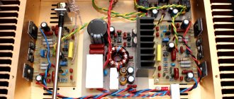
The figure above shows the circuit diagram of a ±56V power supply, and this is nothing new. As always, I recommend a 400 V/35 A diode bridge mounted on a radiator.
Filter capacitors must be rated (at a minimum) for the rated supply voltage, and preferably higher. If possible, use 105°C capacitors.
Note
. The fuse should be selected according to the size of the power transformer. For any toroidal transformer above 300W, a soft starting circuit is highly recommended. Use a fuse recommended by the transformer manufacturer.
The DC source must be taken from the capacitor terminals and not from the diode bridge. Using several small capacitors will give better performance than one large one, and is usually cheaper. For example, the performance of 10 1000uF capacitors is much better (in every way) than one 10,000uF capacitor.
By purchasing a PCB, you will not only get all the component values, but you will also have access to information for a power supply optimized for the best performance for a conventional power supply.
Testing
Connect to a suitable power source - remember the ground must be connected! When first powering up, use 10 to 22 ohm "protection" resistors in series with each power supply to limit the current if you make a wiring mistake.
Translation: LDS, especially for ldsound.ru
As of December 2022, the PCB costs $20.
Project Author: Rod Elliott Elliott Sound Products
Parts and replacements
Field-effect transistors for the first stage must be selected according to the cutoff voltage (a difference of up to 0.5 V is acceptable) and the initial drain current (currents can differ by no more than 25%).
In addition to those indicated in the diagram, any transistors of the KP302, K303, KP307 series (V1, V2) can be used in the preamplifier; KT342 and KT373 with indices A, B, D (V3, V4); KT203A, KT502F - KT502E, KT361V - KT361E (V5) KT601A, KT503G - KT503E, KT315V - KT315E (V6). When using transistors of the KT315 and KT361 series, it is recommended to reduce the supply voltage to ± 20 V. Diodes V7, V8 - any low-power silicon. For power supply, a source with a ripple voltage of no more than 5 mV is required.
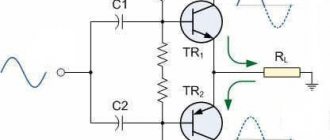
ULF circuits for working with low-Ohm loads
Basic amplifier parameters
Typical ULFs, designed to operate with low-impedance loads and having an output power of tens of mW and higher, are shown in Fig. 16, 17.
Rice. 16. A simple ULF for working with a low-resistance load.
Electrodynamic head BA1 can be connected to the output of the amplifier, as shown in Fig. 16, or diagonally to the bridge (Fig. 17). If the power source is made of two series-connected batteries (accumulators), the right output of the head BA1 according to the diagram can be connected to their midpoint directly, without capacitors C3, C4.
Rice. 17. Circuit of a low-frequency amplifier with the inclusion of a low-resistance load in the diagonal of the bridge.
If you need a circuit for a simple tube ULF, then such an amplifier can be assembled even using one tube, look at our electronics website in the corresponding section.
Literature: Shustov M.A. Practical circuit design (Book 1), 2003.
Corrections in the publication: in Fig. 16 and 17, instead of diode D9, a chain of diodes is installed.
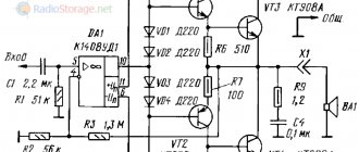
5.5. Collector stabilization circuit
In a circuit with collector stabilization, there is no resistance in the emitter circuit: RE = 0, Fig. 5.6, and the circuit input and output are connected by resistance RB.
Rice. 5.6. Collector stabilization circuit
The bias current in this circuit is:
;
and decreases with increasing (change - in the general case). This is where OOC manifests itself; in terms of the method of removal and insertion, this is a parallel OOS. The depth of this feedback is:
; (5.4)
This circuit is simple, provides mode stabilization up to 30°C, but has a significant drawback - due to the negative feedback on alternating current through resistance RB, low gain. To do this, an RC filter is included in the base circuit, which eliminates the negative feedback on alternating current.