A simple transistor amplifier can be a good tool for studying the properties of devices. The circuits and designs are quite simple; you can make the device yourself and check its operation, take measurements of all parameters. Thanks to modern field-effect transistors, it is possible to make a miniature microphone amplifier from literally three elements. And connect it to a personal computer to improve sound recording parameters. And the interlocutors during conversations will hear your speech much better and more clearly.
Frequency characteristics
Low (audio) frequency amplifiers are found in almost all household appliances - stereo systems, televisions, radios, tape recorders, and even personal computers. But there are also RF amplifiers based on transistors, lamps and microcircuits. The difference between them is that the ULF allows you to amplify the signal only at the audio frequency that is perceived by the human ear. Transistor audio amplifiers allow you to reproduce signals with frequencies in the range from 20 Hz to 20,000 Hz.
Consequently, even the simplest device can amplify the signal in this range. And it does this as evenly as possible. The gain depends directly on the frequency of the input signal. The graph of these values is almost a straight line. If a signal with a frequency outside the range is applied to the amplifier input, the quality of operation and efficiency of the device will quickly decrease. ULF cascades are assembled, as a rule, using transistors operating in the low and mid-frequency ranges.
Classes of operation of audio amplifiers
All amplifying devices are divided into several classes, depending on the degree of current flow through the cascade during the period of operation:
- Class “A” - current flows non-stop during the entire period of operation of the amplifier stage.
- In work class "B" current flows for half a period.
- Class “AB” indicates that current flows through the amplifier stage for a time equal to 50-100% of the period.
- In mode “C”, electric current flows for less than half the operating time.
- ULF mode “D” has been used in amateur radio practice quite recently - a little over 50 years. In most cases, these devices are implemented on the basis of digital elements and have a very high efficiency - over 90%.
The presence of distortion in various classes of low-frequency amplifiers
The working area of a class “A” transistor amplifier is characterized by fairly small nonlinear distortions. If the incoming signal spits out higher voltage pulses, this causes the transistors to become saturated. In the output signal, higher ones begin to appear near each harmonic (up to 10 or 11). Because of this, a metallic sound appears, characteristic only of transistor amplifiers.
If the power supply is unstable, the output signal will be modeled in amplitude near the network frequency. The sound will become harsher on the left side of the frequency response. But the better the stabilization of the amplifier's power supply, the more complex the design of the entire device becomes. ULFs operating in class “A” have a relatively low efficiency - less than 20%. The reason is that the transistor is constantly open and current flows through it constantly.
To increase (albeit slightly) efficiency, you can use push-pull circuits. One drawback is that the half-waves of the output signal become asymmetrical. If you transfer from class “A” to “AB”, nonlinear distortions will increase by 3-4 times. But the efficiency of the entire device circuit will still increase. ULF classes “AB” and “B” characterize the increase in distortion as the signal level at the input decreases. But even if you turn up the volume, this will not help completely get rid of the shortcomings.
↑ Possible modernization
1. Transistors of the KT814 type inserted into the sockets “look” with inscriptions from the user. To eliminate this, you need to mirror the printed circuit board design from right to left.
2. If the KB junction is broken, the zener diode TL431 will receive voltage without a limiting resistor. Therefore, questionable transistors must first be checked for short circuits using a tester ohmmeter. To protect the TL431, instead of a 100 kOhm resistor (it prevents the mode with the base being torn off, I installed it to be on the safe side) you can install a 100 Ohm resistor and connect it in series with the milliammeter.
3. When an increased supply voltage is supplied for a long time, the power on the ballast resistor TL431 exceeds the rated value. You have to manage to burn out the resistor, but if you have such talent, you can install it with a power of 0.5 W with a resistance of 200 Ohms.
I did not make these changes - I consider it unnecessary to make “foolproof” for myself in a circuit of one zener diode and several resistors. The board is simply glued to a piece of foam with a rigid film. It looks unaesthetic, but it works, it suits me, as they say: “cheap, reliable and practical.”
Work in intermediate classes
Each class has several varieties. For example, there is a class of amplifiers “A+”. In it, the input transistors (low voltage) operate in mode “A”. But high-voltage ones installed in the output stages operate either in “B” or “AB”. Such amplifiers are much more economical than those operating in class “A”. A noticeably smaller number of nonlinear distortions is not higher than 0.003%. Better results can be achieved using bipolar transistors. The operating principle of amplifiers based on these elements will be discussed below.
But there is still a large number of higher harmonics in the output signal, causing the sound to become characteristically metallic. There are also amplifier circuits operating in class “AA”. In them, nonlinear distortions are even less - up to 0.0005%. But the main drawback of transistor amplifiers still exists - the characteristic metallic sound.
"Alternative" designs
This is not to say that they are alternative, but some specialists involved in the design and assembly of amplifiers for high-quality sound reproduction are increasingly giving preference to tube designs. Tube amplifiers have the following advantages:
- Very low level of nonlinear distortion in the output signal.
- There are fewer higher harmonics than in transistor designs.
But there is one huge disadvantage that outweighs all the advantages - you definitely need to install a device for coordination. The fact is that the tube stage has a very high resistance - several thousand Ohms. But the speaker winding resistance is 8 or 4 ohms. To coordinate them, you need to install a transformer.
Of course, this is not a very big drawback - there are also transistor devices that use transformers to match the output stage and the speaker system. Some experts argue that the most effective circuit is a hybrid one - which uses single-ended amplifiers that are not affected by negative feedback. Moreover, all these cascades operate in ULF class “A” mode. In other words, a power amplifier on a transistor is used as a repeater.
Moreover, the efficiency of such devices is quite high - about 50%. But you should not focus only on efficiency and power indicators - they do not indicate the high quality of sound reproduction by the amplifier. The linearity of the characteristics and their quality are much more important. Therefore, you need to pay attention primarily to them, and not to power.
Amplifier circuit.
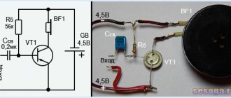
As an experiment, let's assemble a simple amplifier using one transistor and analyze its operation.
To the collector circuit of transistor VT1
Let's turn on the high-resistance electromagnetic telephone
BF2
install a resistor
Rb
between the base and the minus of the power supply
GB , and a decoupling capacitor
Csv
, included in the base circuit of the transistor.
Of course, we will not hear strong amplification from such an amplifier, and to hear the sound in the BF1
it will have to be presented very close to the ear.
Since loud sound reproduction requires an amplifier with at least two or three
transistors or a so-called
two-stage
amplifier.
But to understand the principle of amplification itself, an amplifier assembled on a single transistor or single-stage
amplifier will be enough for us.
Amplifier stage
It is customary to call a transistor with resistors, capacitors and other circuit elements that provide the transistor with operating conditions as an amplifier.
Single-ended ULF circuit on a transistor
The simplest amplifier, built according to a common emitter circuit, operates in class “A”. The circuit uses a semiconductor element with an npn structure. A resistance R3 is installed in the collector circuit, limiting the flow of current. The collector circuit is connected to the positive power wire, and the emitter circuit is connected to the negative wire. If you use semiconductor transistors with a pnp structure, the circuit will be exactly the same, you just need to change the polarity.
Using a decoupling capacitor C1, it is possible to separate the alternating input signal from the direct current source. In this case, the capacitor is not an obstacle to the flow of alternating current along the base-emitter path. The internal resistance of the emitter-base junction together with resistors R1 and R2 represent the simplest supply voltage divider. Typically, resistor R2 has a resistance of 1-1.5 kOhm - the most typical values for such circuits. In this case, the supply voltage is divided exactly in half. And if you power the circuit with a voltage of 20 Volts, you can see that the value of the current gain h21 will be 150. It should be noted that HF amplifiers on transistors are made according to similar circuits, only they work a little differently.
In this case, the emitter voltage is 9 V and the drop in the “E-B” section of the circuit is 0.7 V (which is typical for transistors on silicon crystals). If we consider an amplifier based on germanium transistors, then in this case the voltage drop in the “E-B” section will be equal to 0.3 V. The current in the collector circuit will be equal to that flowing in the emitter. You can calculate it by dividing the emitter voltage by resistance R2 – 9V/1 kOhm=9 mA. To calculate the value of the base current, you need to divide 9 mA by the gain h21 - 9 mA/150 = 60 μA. ULF designs usually use bipolar transistors. Its operating principle is different from field ones.
On resistor R1, you can now calculate the drop value - this is the difference between the base and supply voltages. In this case, the base voltage can be found using the formula - the sum of the characteristics of the emitter and the “E-B” transition. When powered from a 20 Volt source: 20 – 9.7 = 10.3. From here you can calculate the resistance value R1 = 10.3 V/60 μA = 172 kOhm. The circuit contains capacitance C2, which is necessary to implement a circuit through which the alternating component of the emitter current can pass.
If you do not install capacitor C2, the variable component will be very limited. Because of this, such a transistor-based audio amplifier will have a very low current gain h21. It is necessary to pay attention to the fact that in the above calculations the base and collector currents were assumed to be equal. Moreover, the base current was taken to be the one that flows into the circuit from the emitter. It occurs only if a bias voltage is applied to the base output of the transistor.
But it must be taken into account that collector leakage current absolutely always flows through the base circuit, regardless of the presence of bias. In common emitter circuits, the leakage current is amplified by at least 150 times. But usually this value is taken into account only when calculating amplifiers based on germanium transistors. In the case of using silicon, in which the current of the “K-B” circuit is very small, this value is simply neglected.
At first glance, all this is traditional and well known. However, every amp sounds different. What's the matter? But it’s all about the circuit solutions of individual cascades, the quality of the applied elementary base, the choice of modes of active elements, and the design solutions of the devices. But everything is in order.
Input stage
The well-known differential stage is actually not as simple as it seems at first glance. Its quality largely determines such amplifier parameters as the signal-to-noise ratio and the rate of rise of the output voltage, as well as the “zero” offset voltage and the temperature stability of the amplifier.
The requirements for the differential stage are determined by the type of negative feedback (NFB) covering the entire amplifier. When comparing non-inverting, with series OOS (Fig. 2) and inverting, with parallel OOS (Fig. 3) amplifiers, the advantages in linearity are on the side of the latter. The fact is that with a sufficiently large gain of the amplifier without OOS, the voltages at the inverting and non-inverting inputs are almost the same. For example, if a 1 V signal is supplied to the non-inverting input of a non-inverting amplifier, then the same voltage will be at its inverting input. In other words, at the inputs of the amplifier there is an alternating common-mode voltage with an amplitude of 1.4 V. It is easy to notice that the collector-emitter voltages of the transistors of the input differential stage will fluctuate with a swing of 2.8 V. Such parasitic modulation leads to a nonlinear change in the parameters of the transistors per clock with input signal. This entails an increase in distortion, primarily intermodulation, which has an extremely negative effect on sound quality. In an inverting amplifier, the common-mode component is practically zero and the above distortions do not occur.
Hence the first conclusion: the transition from a non-inverting connection to an inverting one significantly improves the sound quality of the amplifier. It is quite easy to carry out such a transition in practice in a finished device. To do this, it is enough to apply a signal from the input connectors to capacitor C2, having previously disconnected it from the zero potential bus of the amplifier, and remove capacitor C1.
| Figure 2. Non-inverting amplifier circuit |
| Figure 3. Inverting amplifier circuit |
The input resistance of the inverting amplifier is almost equal to the resistance of resistor R2. This is much less than the input impedance of a non-inverting amplifier, which is determined by resistor R1. Therefore, in order to keep the frequency response unchanged in the low-frequency region, in some cases it is necessary to increase the capacitance of capacitor C2, which should be as many times greater than the capacitance of capacitor C1 as the resistance of resistor R1 is greater than the resistance of resistor R2. In addition, to keep the gain of the entire device unchanged, you will have to select resistor R3 in the OOS circuit, because the gain of the inverting amplifier is K = R3/R2, and that of the non-inverting amplifier is K = 1 + R3/R2. In this case, to minimize the zero offset voltage at the output, resistor R1 must be selected with the same resistance as the newly installed resistor R3.
If you still need to maintain the non-inverting connection of the first stage, but at the same time eliminate the influence of common-mode distortion, you should increase the output resistance of the current source by replacing resistor R7 in the emitter circuits of the differential stage with a transistor source of stable current (Fig. 4). If such a source is already available in the amplifier, its output resistance can be increased by increasing the value of resistor R14 in the emitter of transistor VT8. At the same time, in order to maintain a constant current through this transistor, the reference voltage at its base should be increased, for example, by replacing the zener diode VD1 with another one with a higher stabilization voltage.
| Figure 4. Stable current source circuit |
A very effective way to reduce amplifier distortion is to use transistors of the same type in the differential stage, pre-selected for static gain and base-emitter voltage.
This method is unacceptable for mass production of amplifiers, but is quite suitable for upgrading single copies of finished devices. Excellent results are obtained by installing a transistor assembly of two transistors in a differential cascade, made in a single technological process on one chip and therefore having close values of the above parameters.
The reduction of distortion is also facilitated by the introduction of local negative current feedback into the first stage of the amplifier by installing resistors with a resistance of up to 100 Ohms (R9, R10) in the emitter circuits of transistors VT1, VT2. In this case, some adjustment of the resistance of resistor R3 in the OOS circuit may be required.
Of course, this does not exhaust all the ways to modernize the input differential stage. It is also possible to install, instead of a single-transistor, a two-transistor current source with record output resistance values, introduce a so-called current mirror in amplifiers with asymmetric signal pickup from the first stage to the voltage amplification stage, switch on each of the transistors in a cascode circuit, etc. However, such alterations are labor-intensive and the design of the amplifier does not always allow them to be performed.
Output stage
The output stage is the main source of distortion in any power amplifier. Its task is to generate an undistorted signal of the required amplitude in the operating frequency range at a low-impedance load.
Let's consider a traditional cascade using complementary pairs of bipolar transistors connected according to a push-pull emitter follower circuit. Bipolar transistors have a capacitance at the emitter-base pn junction, which can reach tenths and hundredths of a microfarad. The size of this capacitance affects the cutoff frequency of the transistors. When a positive half-wave signal is applied to the cascade input, the upper arm of the push-pull cascade (VT4, VT6) operates. Transistor VT4 is connected according to a common collector circuit and has a low output resistance, so the current flowing through it quickly charges the input capacitance of transistor VT6 and opens it. After changing the polarity of the input voltage, the lower arm of the output stage is turned on, and the upper one is turned off. Transistor VT6 closes. But in order to completely turn off the transistor, it is necessary to discharge its input capacitance. It is discharged mainly through resistors R5 and R6, and relatively slowly. By the time the lower arm of the output stage is turned on, this capacitance does not have time to completely discharge, so the transistor VT6 does not close completely, and the collector current of the transistor VT6, in addition to its own, flows through the transistor VT7. As a result, due to the occurrence of through current at high frequencies at high switching speeds, not only does the power dissipated by transistors increase and the efficiency decreases, but signal distortion also increases. The simplest way to eliminate the described drawback is to reduce the resistance of resistors R5 and R6. However, this increases the power dissipated by transistors VT4 and VT5. A more rational way to reduce distortion is to change the circuit of the amplifier's output stage in such a way as to force the resorption of excess charge (Fig. 5). This can be achieved by connecting resistor R5 to the emitter of transistor VT5.
| Figure 5. Diagram of amplifier output stages |
In the case of high output resistance of the pre-terminal stage, excess charge can accumulate on the bases of transistors VT4 and VT5. To eliminate this phenomenon, it is necessary to connect the bases of these transistors to the zero potential point of the amplifier through resistors R11 and R12 with ratings of 10...24 kOhm.
The measures described are quite effective. Compared to a typical connection, the rate of decrease in the collector current in the output stage after the described modifications is approximately four times greater, and the distortion at a frequency of 20 kHz is approximately three times less.
From the point of view of introduced distortions, the limiting cutoff frequency of the transistors used, as well as the dependence of their static current gain and cutoff frequency on the emitter current, is very important. Therefore, further improvement in the quality performance of amplifiers with an output stage based on bipolar transistors can be achieved by replacing the output transistors with higher-frequency ones with a lesser dependence of the gain on the emitter current. As such transistors, we can recommend complementary pairs 2SA1302 and 2SC3281; 2SA1215 and 2SC2921; 2SA1216 and 2SC2922. All transistors are manufactured by Toshiba in TO-247 packages.
To a large extent, the sound quality of an amplifier is influenced by its ability to operate with a low-impedance load, i.e. deliver the maximum signal current to the load without distortion.
It is known that any acoustic system (abbreviated as AC) is characterized by an output complex impedance module Z. Typically, the value of this resistance is indicated in the passports of serial household speakers and is 4 or 8 Ohms. However, this is only true at one frequency, usually 1 kHz. In the range of operating frequencies, the module of the complex resistance changes several times and can decrease to 1...2 Ohms. In other words, for non-periodic, wide-spectrum pulsed signals, such as a music signal, the speaker presents a low-impedance load for the amplifier that many commercial amplifiers simply cannot handle.
Therefore, the most effective way to improve the quality indicators of the output stage when working with a real complex load is to increase the number of transistors in the arms of a push-pull amplifier. This allows not only to increase the reliability of the amplifier, since the area of safe operation of each transistor expands, but, most importantly, to reduce distortion due to the redistribution of collector currents between transistors. In this case, the range of variation of the collector current and, accordingly, the gain is narrowed, which leads to a decrease in distortion on a low-impedance load, of course, subject to certain requirements for the power source.
A completely radical way to radically improve the sound of an amplifier is to replace the bipolar transistors in the output stage with insulated-gate field-effect transistors (MOSFETs).
| Figure 6. Circuit diagram of the output stage of an amplifier using field-effect transistors |
Compared to bipolar MOSFETs, they are distinguished by better linearity of pass-through characteristics and significantly higher operating speed, i.e. better frequency properties. These features of field-effect transistors, when used, allow relatively simple means to bring the parameters and sound quality of the upgraded amplifier to the highest level, which has been repeatedly confirmed in practice. Improving the linearity of the output stage is also facilitated by such a feature of field-effect transistors as a high input resistance, which makes it possible to do without a pre-final stage, usually performed using a Darlington circuit, and further reduce distortion by shortening the signal path.
The absence of the phenomenon of secondary thermal breakdown in field-effect transistors expands the area of safe operation of the output stage and thereby makes it possible to increase the reliability of the amplifier as a whole, and also, in some cases, to simplify the circuits for temperature stabilization of the quiescent current.
Of course, installing field-effect transistors instead of bipolar ones requires some modernization of the initial bias circuits of the output stage transistors. This modernization comes down to replacing the values of resistors R17…R19. This is necessary due to the significantly higher unlocking voltage at the gate of the field-effect transistor compared to the unlocking voltage based on the bipolar transistor. It is also necessary to correct the quiescent current of the pre-output stage, which must be of sufficient magnitude to quickly recharge the large input capacitances of MOSFETs, significantly larger than those of bipolar transistors. A current value of 10 mA is usually sufficient for practical purposes. In some cases, when increasing the quiescent current specified by the amplifier manufacturer, it will be necessary to install additional radiators on the transistors of the pre-output stage. In addition, it is necessary to install anti-parasitic resistors with a resistance of 200...470 Ohms in the gate circuit of each field-effect transistor. Without these resistors or with a smaller value, the amplifier is self-excited. As output stage transistors, we can recommend complementary pairs IRFP240, IRFP9240 from InternationalRectifier and 2SK1530, 2SJ201 in TO-247 packages from Toshiba.
And one last thing. To increase the reliability of the amplifier, it would not be superfluous to install protective zener diodes VD3, VD4 with a stabilization voltage of 10...15 V in the transistor gate circuit. These zener diodes will protect the gate from breakdown, the reverse breakdown voltage of which usually does not exceed 20 V.
When analyzing the circuits for setting the initial bias of the output stage of any amplifier, you should pay attention to two points.
The first point is related to what initial quiescent current is set. Many foreign manufacturers set it within 20...30 mA, which is clearly not enough from the point of view of high-quality sound at low volume levels. Although there are no visible “step” distortions in the output signal, insufficient quiescent current leads to a deterioration in the frequency properties of the transistors, and as a result, to an unintelligible, “dirty” sound at low volume levels, and “blurring” of small details. The optimal value of the quiescent current should be considered 50...100 mA. If the amplifier has several transistors in the arm, then this value applies to each transistor. In the vast majority of cases, the area of the amplifier's radiators allows long-term heat removal from the output transistors at the recommended quiescent current value.
The second, very important point is that the high-frequency transistor, often used in the classical scheme for installing and thermally stabilizing the quiescent current, is excited at high frequencies, and its excitation is very difficult to detect. Therefore, it is advisable to use a low-frequency transistor with ft instead. In any case, replacing this transistor with a low-frequency one guarantees against troubles. The inclusion of a capacitor C4 with a capacity of up to 0.1 μF between the collector and base also helps to eliminate dynamic voltage changes.
Frequency correction of power amplifiers
The most important condition for ensuring high-quality sound reproduction is to reduce the dynamic distortion of the transistor amplifier to the minimum possible. In amplifiers with deep feedback, this can be achieved by paying serious attention to frequency correction. As is known, a real audio signal has a pulsed nature, therefore, a sufficient idea for practical purposes about the dynamic properties of an amplifier can be obtained from its response to a jump in input voltage, which, in turn, depends on the transient response. The latter can be described using the attenuation coefficient. The transient characteristics of amplifiers for various values of this coefficient are shown in Fig. 7.
| Figure 7. Transient characteristics of amplifiers |
Based on the magnitude of the first surge in the output voltage Uout = f(t), one can make an unambiguous conclusion about the relative stability of the amplifier. As can be seen from the figures shown. 7 characteristics, this surge is maximum at low attenuation coefficients. Such an amplifier has a small margin of stability and, other things being equal, has large dynamic distortions, which manifest themselves in the form of “dirty”, “opaque” sound, especially at high frequencies of the audible sound range.
From the point of view of minimizing dynamic distortion, the most successful amplifier is one with an aperiodic transient response (attenuation coefficient less than 1). However, it is technically very difficult to implement such an amplifier in practice. Therefore, most manufacturers make a compromise by providing a lower attenuation coefficient.
In practice, optimization of frequency correction is carried out as follows. By applying a square wave signal with a frequency of 1 kHz from the pulse generator to the input of the amplifier and observing the transient process at the output using an oscilloscope, selecting the capacitance of the correction capacitor to achieve a shape of the output signal that is closest to rectangular.
Effect of amplifier design on sound quality
In well-designed amplifiers, with carefully designed circuitry and operating modes of active elements, unfortunately, design issues are not always thought through. This leads to the fact that signal distortion caused by installation interference from the output stage currents to the input circuits of the amplifier makes a noticeable contribution to the overall level of distortion of the entire device. The danger of such interference is that the shapes of the currents passing through the power circuits of the arms of a push-pull output stage operating in class AB mode are very different from the shapes of the currents in the load.
If interference from these currents enters the input circuits, noticeable distortion occurs, especially at high frequencies, at which parasitic couplings increase.
To combat this phenomenon, it is necessary to minimize the parasitic inductance of high-current amplifier circuits. In a ready-made design, this can be achieved by installing additional smaller capacitors along the power supply circuits of the output stage, connected in parallel with the rectifier filter capacitors. In this case, additional capacitors should be located physically as close as possible to consumers, i.e. transistors of the amplifier output stage. The best option is to install one capacitor directly at the collector or drain terminal of each output transistor. It would not be superfluous to shunt newly installed oxide electrolytic capacitors with film capacitors, preferably with a dielectric made of polypropylene or polystyrene.
The second design reason for increased amplifier distortion is poor routing of ground buses on the printed circuit board. Due to the insufficient cross-section on the buses, a noticeable voltage drop occurs, created by currents in the power circuits of the output stage. As a result, the ground potentials of the input stage and the ground potentials of the output stage become different. A so-called distortion of the “reference potential” of the amplifier occurs. This constantly changing potential difference is added to the voltage of the desired signal at the input and amplified by subsequent stages of the amplifier, which is equivalent to the presence of interference and leads to an increase in harmonic and intermodulation distortions.
To combat such interference in the finished amplifier, it is necessary to connect the zero potential buses of the input stage, the zero load potential and the zero potential of the power supply at one point (star) with wires of a sufficiently large cross-section. But the most radical way to eliminate reference potential distortion is to galvanically isolate the common wire of the amplifier input stage from a powerful power bus. This solution is possible in an amplifier with a differential input stage. Only the terminals of resistors R1 and R2 are connected to the common wire of the signal source (on the left in the diagram in the figure. All other conductors connected to the common wire are connected to the powerful power supply bus, on the right in the diagram. However, in this case, the shutdown for some reason signal source can lead to the failure of the amplifier, since the left "ground" bus is not connected to anything and the state of the output stage becomes unpredictable. To avoid an emergency situation, both "ground" buses are connected to each other by resistor R4. Its resistance should not exceed very small so that interference from a powerful power bus cannot reach the amplifier input, and at the same time not too large so as not to affect the depth of feedback.In practice, the resistance of resistor R4 is about 10 Ohms.
| Figure 8. Isolation of the common wire of the amplifier input stage from the powerful power bus |
Energy consumption of the power supply
In the vast majority of industrial amplifiers, the capacity of the storage (filtering) capacitors of the power supply is clearly insufficient, which is explained solely by economic reasons, because electrical capacitors of large values (from 10,000 μF or more) are clearly not the cheapest components. Insufficient capacitance of filter capacitors leads to “squeezed” dynamics of the amplifier and an increase in the background level, i.e. to deterioration of sound quality. The author's practical experience in the field of upgrading a large number of different amplifiers indicates that “real sound” begins with a power supply energy intensity of at least 75 J per channel. To ensure such energy intensity, a total capacitance of filter capacitors of at least 45,000 μF is required at a supply voltage of 40 V per arm (E = CU2/2).
Quality of the element base
Not the least role in ensuring high sound quality of amplifiers is played by the quality of the element base, mainly passive components, i.e. resistors and capacitors, as well as installation wires.
And if most manufacturers use permanent carbon and metal film resistors of fairly high quality in their products, the same cannot be said for permanent capacitors. The desire to save on product costs often leads to disastrous results. In those circuits where it is necessary to use high-quality polystyrene or polypropylene film capacitors with low dielectric losses and a low dielectric absorption coefficient, penny oxide capacitors or, somewhat better, capacitors with a dielectric made of Mylar (polyethylene terephthalate) film are often installed. Because of this, even well-designed amplifiers sound “unintelligible” and “muddy”. When playing musical fragments, there are no sound details, the tonal balance is disturbed, and there is clearly a lack of speed, which is manifested in the sluggish attack of the sound of musical instruments. Other aspects of the sound suffer as well. Overall the sound leaves much to be desired.
Therefore, when upgrading truly high-quality amplification devices, it is necessary to replace all low-quality capacitors. Good results are obtained by using capacitors from Siemens, Philips, and Wima. When fine-tuning expensive high-end devices, it is best to use capacitors from the American company Reelcup, types PPFX, PPFX-S, RTX (types are listed in ascending order of cost).
Last but not least, you should pay attention to the quality of the rectifier diodes and mounting wires.
Powerful rectifier diodes and rectifier bridges, which are widely used in amplifier power supplies, have low performance due to the effect of resorption of minority charge carriers in the pn junction. As a result, when the polarity of the AC voltage supplied to the rectifier is changed, the diodes that are in the open state close with some delay, which in turn leads to the appearance of powerful impulse noise. Interference penetrates through the power supply circuits into the audio path and degrades the sound quality. To combat this phenomenon, it is necessary to use high-speed pulsed diodes, and even better, Schottky diodes, in which the effect of resorption of minority charge carriers is absent. Of the available ones, we can recommend diodes from International Rectifier. As for the installation wires, it is best to replace the existing conventional installation wires with large-gauge oxygen-free copper cables. First of all, you should replace the wires that transmit the amplified signal to the output terminals of the amplifier, the wires in the power circuits, and, as necessary, the wiring from the input jacks to the input of the first amplifier stage.
It is difficult to give specific recommendations on cable brands. It all depends on the taste and financial capabilities of the amplifier owner. Among the well-known and available cables on our market, we can recommend cables from Kimber Kable, XLO, Audioquest.
Repair of electronic equipment No. 3 2002
Amplifiers based on MOS transistors
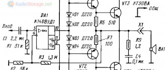
The field-effect transistor amplifier shown in the diagram has many analogues. Including using bipolar transistors. Therefore, we can consider, as a similar example, the design of an audio amplifier assembled according to a circuit with a common emitter. The photo shows a circuit made according to a common source circuit. RC connections are assembled on the input and output circuits so that the device operates in class “A” amplifier mode.
The alternating current from the signal source is separated from the direct supply voltage by capacitor C1. The field-effect transistor amplifier must necessarily have a gate potential that will be lower than the same source characteristic. In the diagram shown, the gate is connected to the common wire via resistor R1. Its resistance is very high - resistors of 100-1000 kOhm are usually used in designs. Such a large resistance is chosen so that the input signal is not shunted.
This resistance almost does not allow electric current to pass through, as a result of which the gate potential (in the absence of a signal at the input) is the same as that of the ground. At the source, the potential turns out to be higher than that of the ground, only due to the voltage drop across resistance R2. From this it is clear that the gate has a lower potential than the source. And this is exactly what is required for the normal functioning of the transistor. It is necessary to pay attention to the fact that C2 and R3 in this amplifier circuit have the same purpose as in the design discussed above. And the input signal is shifted relative to the output signal by 180 degrees.
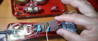
Printed circuit boards for assembly
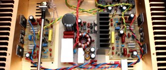
24 V power supply and protection. The power supply supplies voltage to control the relay. To avoid unpleasant sound effects when turning on / off the amplifier, protection has been added in the form of a delay in turning on and immediately turning off the speakers and protection against the occurrence of constant voltage at the speaker output. Two relays allow you to connect two loudspeakers.
Everything is assembled in the original case from the ULF.
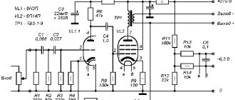
ULF with transformer at the output
You can make such an amplifier with your own hands for home use. It is carried out according to the scheme that works in class “A”. The design is the same as those discussed above - with a common emitter. One feature is that you need to use a transformer for matching. This is a disadvantage of such a transistor-based audio amplifier.
The collector circuit of the transistor is loaded by the primary winding, which develops an output signal transmitted through the secondary to the speakers. A voltage divider is assembled on resistors R1 and R3, which allows you to select the operating point of the transistor. This circuit supplies bias voltage to the base. All other components have the same purpose as the circuits discussed above.
↑ Technical specifications
As always, I believe that an amateur design, as a rule, should be simple, cheap, technologically advanced, and consist of non-scarce parts. In addition, I long ago came to the conclusion that for such purposes it is better to make small simple boards without a power supply, without a digital indicator, without a complex case. It is enough to provide clamps for connecting an external laboratory regulated power supply, an indicator in the form of a simple digital tester or pointer instrument, and, if necessary, an oscilloscope, etc.
Such devices are quickly made and remade, and most importantly, they work and are useful. If you think of a multifunctional, self-sufficient device in a separate beautiful case, it will usually remain in the spotlights. In addition, if the device is made, it suddenly turns out that it is necessary to add another function, for example, a capacitance viewer, but there is no more space on the front panel and the design must be spoiled... Therefore, I believe that unsightly amateur narrowly functional products have a right to life.
So, it is planned to test silicon transistors in the mode - current 200 mA, voltage K-E = 2 V. You can quickly change the current in the range of approximately 150...300 mA, voltage K-E up to 5...7 V. You can check (by slightly changing the settings) composite transistors with two serial PN junctions.
Using a toggle switch you can change the current, for example, 10 times. This will allow you to test low-power transistors at a current of 15...30 mA (by replacing one resistor you can set any reasonable current). I think it’s important to connect any transistors conveniently. For transistors KT814-819 there are sockets on the board, for powerful transistors in cases like TO-247, TO-3R, there are clamps. They install wires with “crocodiles”, which allow you to connect transistors in the TO-3 housing, any transistors with bent solder leads, etc.
The change in the C-E voltage is carried out by an external power source, the goal is to check the identity of the modes at higher voltages and significant heating of the transistors. At 5 V and 200 mA, we get the maximum power for KT814 without a heat sink - 1 W. For larger cases without heatsinks, thermal power is typically = 2 W.
It is easy to see that the transistor gain depends to some extent on both voltage and temperature, so determining the absolute value of the transistor gain using a microprocessor with an accuracy of up to the seventh digit does not make sense. For this reason, the simplest circuit solution was chosen, which provides sufficient accuracy for practice and allows you to do without an op-amp, microcontroller and several power supplies. Any digital tester, for example M-832, is suitable for measuring the base current.
Push-pull audio amplifier
It cannot be said that this is a simple transistor amplifier, since its operation is a little more complicated than those discussed earlier. In push-pull ULFs, the input signal is split into two half-waves, different in phase. And each of these half-waves is amplified by its own cascade, made on a transistor. After each half-wave has been amplified, both signals are combined and sent to the speakers. Such complex transformations can cause signal distortion, since the dynamic and frequency properties of two transistors, even of the same type, will be different.
As a result, the sound quality at the amplifier output is significantly reduced. When a push-pull amplifier operates in class “A”, it is not possible to reproduce a complex signal with high quality. The reason is that an increased current constantly flows through the amplifier’s shoulders, the half-waves are asymmetrical, and phase distortions occur. The sound becomes less intelligible, and when heated, signal distortion increases even more, especially at low and ultra-low frequencies.
Transformerless ULF
A transistor-based bass amplifier made using a transformer, despite the fact that the design may have small dimensions, is still imperfect. Transformers are still heavy and bulky, so it's better to get rid of them. A circuit made on complementary semiconductor elements with different types of conductivity turns out to be much more effective. Most modern ULFs are made precisely according to such schemes and operate in class “B”.
The two powerful transistors used in the design operate according to an emitter follower circuit (common collector). In this case, the input voltage is transmitted to the output without loss or gain. If there is no signal at the input, then the transistors are on the verge of turning on, but are still turned off. When a harmonic signal is applied to the input, the first transistor opens with a positive half-wave, and the second one is in cutoff mode at this time.
Consequently, only positive half-waves can pass through the load. But the negative ones open the second transistor and completely turn off the first. In this case, only negative half-waves appear in the load. As a result, the signal amplified in power appears at the output of the device. Such an amplifier circuit using transistors is quite effective and can provide stable operation and high-quality sound reproduction.
↑ Background
In the manufacture of amateur designs, especially amplifiers, it is highly desirable that pairs of transistors, both of the same conductivity and complementary, have as close parameters as possible. All other things being equal, transistors selected for current transfer coefficient work better, especially in the era of fashion for amplifiers with shallow OOS or even without it. Modern industrial devices are too expensive and not designed for hobbyists, and old ones are ineffective. The transistor meters built into cheap digital testers are not suitable for this purpose at all, since they usually carry out measurements at a current of 1 mA and a voltage of 5 V. Searches on the Internet for a simple but functional design did not yield any results, so once again I have to do the selection “on my knees” I don’t want it anymore, I want comfort. I had to invent it myself. I hope that there will be people willing to repeat this design.
ULF circuit on one transistor
Having studied all the features described above, you can assemble the amplifier with your own hands using a simple element base. The transistor can be used domestic KT315 or any of its foreign analogues - for example BC107. As a load, you need to use headphones with a resistance of 2000-3000 Ohms. A bias voltage must be applied to the base of the transistor through a 1 MΩ resistor and a 10 μF decoupling capacitor. The circuit can be powered from a source with a voltage of 4.5-9 Volts, a current of 0.3-0.5 A.
If resistance R1 is not connected, then there will be no current in the base and collector. But when connected, the voltage reaches a level of 0.7 V and allows a current of about 4 μA to flow. In this case, the current gain will be about 250. From here you can make a simple calculation of the amplifier using transistors and find out the collector current - it turns out to be equal to 1 mA. Having assembled this transistor amplifier circuit, you can test it. Connect a load to the output - headphones.
Touch the amplifier input with your finger and a characteristic noise should appear. If it is not there, then most likely the structure was assembled incorrectly. Double-check all connections and element ratings. To make the demonstration more clear, connect a sound source to the ULF input - the output from a player or phone. Listen to music and evaluate the sound quality.
Selection of transistors for the JLH amplifier
Output transistors
- Old copies that were made using mesa-planar technology (2N3055), which was replaced by modern epitaxial-palar technology (MJE3055) are very musical transistors.
- Despite the frequency response, the sound of the 2n3055 is louder and more transparent, but the sound of the 2sc3281 is more muffled and tube-like, or something. Apparently, the distribution of harmonics affects
- The best and most stable in this unit still turned out to be MJ15024, MJ15003, 2N2773. The BAT of the output stage transistors at a 4 Ohm load should be at least 120.
- Super transistors - MJ15026, 15027 for $27 one, in the States $7.
Well, the Motorola clone 2SC3281 is MJL3281A, it is generally a record holder in terms of Kus linearity. Almost a straight “shelf”, and the decline in beta begins at 5-6 Amps. In terms of sound, the leaders are MJL3281A (NPN) MJL1302A (PNP) as the most integrally linear powerful bipolar transistors for AF.
A very good result is obtained by parallel connection at the output of 2 3 medium power transistors 2sc5707, pre-selected by betta (they have a very high one - up to 560). We solder 2-3 transistors onto a common copper plate, and then attach it to the radiator through a gasket; it is better to solder with low-melting solder pos-61.
In plastic (TO-247) you can install MJE21193, 2CS5200, KT8101 (in order of quality deterioration); In metal (TO-3) you can use MJ15003, MJ15024, 2N3055, KT819VM, GM (in the same order); Of ours - KT908, KT903, KT808, KT805, KT803 (KT908 is head and shoulders above all others, among the domestic ones they are the best).
Do not use MJL21294, these transistors are not for this amplifier. Especially with a 4 ohm load. This is where they belong in Igor Semynin’s single-cycle repeater or amplifiers with composite transistors at the output. In an amplifier according to the JLH circuit, the higher the voltage of the output transistors and the pre-output transistor, the better. MJL-21194 is now the best for sound but not for Hood, JLH can use MJ15003, but their body is uncomfortable, like 2N3055
I looked at the characteristics of the device on this set of transistors: High-frequency output 2sc5200 + driver stage at VS550bp, input transistor bc109b. The distortion turned out to be 0.02. 0.03% with an excellent meander. Under the same conditions, low-frequency motorolas with a low beta give distortion of 0.08-0.1% with a strongly blocked meander front.
A circuit with RF transistors at the output must necessarily be corrected from excitation by installing capacitors between the base and collector of the driver transistor of the order of 10-15 pF and a capacitor with a capacity of 22-60 pF in parallel with the OOS resistor R5 2.7 kOhm. If the OOS capacitor has a rating of 470-680 μF, then the OOS divider 2.7 kOhm/240 Ohm is better reduced to 1.2 kOhm/120 Ohm, which will give less distortion and greater stability.
Modern transistors are inferior to vintage ones in terms of bass reproduction quality. I find the 2SA1943, 2SC5200 to provide better sound than the MJ15003, 15004 or MJ15024, 25.
MJL21194 combine the advantages: a flat, easy-to-install case and a narrow band of 4-6.5 MHz. True, they have two “minuses” - high cost and low gain. It is not recommended to install powerful modern transistors with ft>30MHz - it will excite. Old low-frequency transistors behave better than new high-frequency transistors. In this sense, it’s worth trying our Kt805-Kt819
For transistors of the series: MJ, MJL, MJW - 21193, 21194, 21195, 21196... copper metallization is used on the surface of the crystal to form the base terminal, which equalizes the temperature of the crystal surface, improves the current distribution over the crystal area and expands the OBR, especially in the high voltage range .
Driver transistor
I tried many transistors in the driver, the 2sc2240 showed the best results, which is natural because it has 300-700 batts, with excellent collector current linearity in the range of 1.0-50 mA and a small capacitance of 3 pF, glue a copper plate to it and we get an excellent medium-power driver = Ibuki
If you have output transistors with a large betta, then the current from the driver transistor is not very large, 15-25 mA, so there is no need to put a stupid horse transistor there. Of the Soviet ones, KT602B is not bad, but it needs to be selected with beta at a current of 20-30 mA of at least 200.
The low-power pre-output transistor shows much better results in terms of meander quality and distortion than the BD139 and the same “medium-power” ones due to more linear characteristics at currents of 10-30 mA, high h21e and small interelectrode capacitances. The quality increase in the classic 1969 scheme is especially good.