Hello dear readers of the site. We continue to master the bipolar transistor and today we will look at its operation in amplification mode using the example of a simple audio amplifier assembled on a single transistor.
In boost mode
transistors operate in circuits of radio broadcast receivers and audio frequency amplifiers (AF).
During operation, small currents in the base
circuit of the transistor are used to control large currents in
the collector
circuit.
This is what distinguishes the amplification mode from the switching mode, which only opens or closes the transistor under the influence of voltage Ub
at the base.
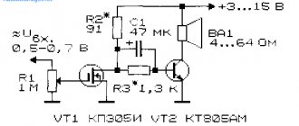
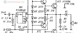
Amplifier circuit.
As an experiment, let's assemble a simple amplifier using one transistor and analyze its operation.
To the collector circuit of transistor VT1
Let's turn on the high-resistance electromagnetic telephone
BF2
install a resistor
Rb
between the base and the minus of the power supply
GB , and a decoupling capacitor
Csv
, included in the base circuit of the transistor.
Of course, we will not hear strong amplification from such an amplifier, and to hear the sound in the BF1
it will have to be presented very close to the ear.
Since loud sound reproduction requires an amplifier with at least two or three
transistors or a so-called
two-stage
amplifier.
But to understand the principle of amplification itself, an amplifier assembled on a single transistor or single-stage
amplifier will be enough for us.
Amplifier stage
It is customary to call a transistor with resistors, capacitors and other circuit elements that provide the transistor with operating conditions as an amplifier.
What is an operational amplifier
Operational amplifier (op-amp) English.
Operational Amplifier (OpAmp), popularly known as an operational amplifier, is a direct current amplifier (DCA) with a very high gain. The phrase "DC amplifier" does not mean that the op amp can only amplify DC current. This means, starting from a frequency of zero Hertz, and this is direct current. The term “operational” has been strengthened for a long time, since the first samples of op-amps were used for various mathematical operations such as integration, differentiation, summation, etc. The gain factor of an op-amp depends on its type, purpose, structure and can exceed 1 million!
Operation of the amplifier circuit.
When supply voltage is supplied to the circuit, to the base of the transistor through resistor Rb
a small negative voltage of 0.1 - 0.2V is supplied, called
offset voltage
.
This voltage slightly opens
the transistor, and a small current begins to flow through the emitter and collector junctions, which, as it were, puts the amplifier into standby mode, from which it will instantly exit as soon as an input signal appears at the input.
Without initial
bias voltage, the emitter pn junction will be
closed
and, like a diode, “
cut off
” the positive half-cycles of the input voltage, causing the amplified signal to be distorted.
If you connect another BF1
and use it as a microphone, the phone will convert sound vibrations into alternating audio frequency voltage, which will be supplied to the base of the transistor through the capacitor
CSV
.
Here, capacitor CSV
acts as a connecting element between the
BF1
and the base of the transistor.
It perfectly passes audio frequency voltage, but blocks the path of direct current from the base circuit to the BF1
. And since the telephone has its own internal resistance (about 1600 Ohms), without this capacitor the base of the transistor through the internal resistance of the telephone would be connected to the emitter via direct current. And naturally, there could be no talk of any signal amplification.
Now, if you start talking into the phone BF1
, then
oscillations in the telephone's electric current
Itlf
emitter-base , which will control the large current in the collector circuit of the transistor.
And
we will hear BF2
The signal amplification process itself can be described as follows. In the absence of input signal voltage Uin
, small currents flow in the base and collector circuits (straight sections of graphs
a
,
b
,
c
), determined by the voltage of the power source, the bias voltage at the base and the amplifying properties of the transistor.
As soon as an input signal appears in the base circuit (the right side of graph a
), then the currents in the transistor circuits begin to change accordingly (the right side of graphs
b
,
c
).
During negative
half-cycles, when the negative input
Uin
and the voltage of the power supply
GB
are summed up at the base - the circuit currents
increase
.
During the positive
half-cycles, when the voltage of the input signal
Uin
and the power supply
GB
are positive, the negative voltage at the base decreases and, accordingly, the currents in both circuits also
decrease
. This is how voltage and current amplification occurs.
If the load of the transistor is not a telephone but a resistor, then the voltage generated on it, the alternating component of the amplified signal, can be fed into the input circuit of the second transistor for additional amplification.
One transistor can amplify the signal 30 to 50 times.
The figure below shows the dependence of the collector current on the base current.
For example. Between points A and B, the base current increased from 50 to 100 μA (microamperes), that is, it amounted to 50 μA, or 0.05 mA. The collector current between these points increased from 3 to 5.5 mA, that is, it increased by 2.5 mA. It follows that the current gain is: 2.5 / 0.05 = 50 times.
NPN structure transistors work in exactly the same way.
.
But for them, the polarity of the power source, base and collector supply circuits is reversed
. That is, positive voltage is applied to the base and collector, and negative voltage is applied to the emitter.
Remember
bias voltage
is necessarily applied to its base, relative to the emitter, along with the
input signal , which opens the transistor.
For germanium
For transistors, the unlocking voltage is no more than 0.2 volts, and for
silicon ones,
no more than 0.7 volts.
The bias voltage is not applied to the base only when the emitter junction of the transistor is used to detect an RF modulated signal.
Stabilization of the transistor operating point
A serious drawback of the circuit in Fig. 1.(b) is that the collector voltage in rest mode depends entirely on the value of hFE of the transistor, while the numerical values of this parameter have a large scatter for different instances of transistors of the same type. For example, with a typical hFE value for transistor BC 107 equal to 200, manufacturers indicate that it can vary from 90 to 450. Changing hFE shifts the DC operating point. For example, if the hFE factor is 100 instead of 200, then a collector current of 0.5 mA will flow rather than 1 mA, and the voltage drop across RL will be only 2.35 V instead of 4.7 V. Increasing the collector voltage by quiescent mode means that the circuit's output voltage can only increase by 2 V, rather than 4 V (it is possible to change the output voltage down to 6 V, but this is of little use when positive increments are limited).
The consequences of using a transistor with hFE = 400 are even more serious. In this case, the collector current will double to 2 mA. A simple calculation shows that all 9V of the supply will drop across resistor RL. The transistor is said to be in saturation. In practice, a small voltage of about 0.2 V remains between the collector and emitter. Any further increase in the base current leads to almost nothing; indeed, the voltage drop across RL cannot exceed Vcc Since when the transistor is saturated, the collector potential is actually equal to the ground potential, the circuit is now not suitable for linear amplification: changes in the output voltage downward are impossible.
Returning to the linear amplifier in Fig. 1.(b), we can say that some improvement of the circuit is necessary to increase its resistance to changes in hFE. Even if we were able to select transistors with hFE = 200, which is very expensive when mass-producing circuits, hFE increases with temperature, so the circuit would still not be reliable. In Fig. 2. a very simple but effective improvement is shown. Instead of connecting resistor RB directly to Vcc, we halve the resistance and connect it to the collector (VCE≈Vcc/2). Now, thanks to this, the base current in quiescent mode depends on the collector voltage in quiescent mode. Even with increasing hFE, the transistor cannot go into saturation: if the collector voltage drops, then the base current also drops, “holding” the collector current. Conversely, if hFE decreases, the quiescent collector voltage increases, increasing the current IB.
The base current is now determined by the relation
IB=VCE/RB
and, as before,
VCE=Vcc-hFEIBRL
Combining these equalities, we get
VCE=Vcc/(1+hFERL/RB)
If RL and RB have the values shown in Fig. 2, and hFE = 100, then VCE≈6 V; if hFE = 400, then VCE ≈3 V. Although the position of the operating point still changes here, this is not significant until obtaining large signals requires the largest possible range of changes in the output voltage. The diagram shown in Fig. 2., will operate when changing transistor parameters over a very wide range and is a useful general purpose voltage amplifier. The hFE self-compensating circuit design is simply an example of negative feedback, which is one of the most important concepts in electronics.
Ideal and real operational amplifier model
In order to understand the essence of the op-amp’s operation, let’s consider its ideal and real models.
1) The input impedance of an ideal op-amp is infinitely large.
In real op-amps, the value of the input resistance depends on the purpose of the op-amp (universal, video, precision, etc.), the type of transistors used and the circuit design of the input stage and can range from hundreds of ohms to tens of megohms. A typical value for a general purpose op amp is a few megohms.
2) The second rule follows from the first rule. Since the input resistance of an ideal op-amp is infinitely large, the input current will be zero.
In fact, this assumption is quite valid for op-amps with field-effect transistors at the input, whose input currents can be less than picoamps. But there are also op-amps with bipolar transistors at the input. Here the input current can already be tens of microamps.
3) The output impedance of an ideal op-amp is zero.
This means that the voltage at the output of the op-amp will not change when the load current changes. In real general-purpose op-amps, the output impedance is tens of ohms (usually 50 ohms). In addition, the output impedance depends on the signal frequency.
4) The gain in an ideal op-amp is infinitely large. In reality, it is limited by the internal circuitry of the op-amp, and the output voltage is limited by the supply voltage.
5) Since the gain is infinitely large, therefore, the voltage difference between the inputs of an ideal op-amp is zero. Otherwise, even if the potential of one input is greater or less than at least the charge of one electron, then the output will have an infinitely large potential.
6) The gain in an ideal op-amp does not depend on the signal frequency and is constant at all frequencies. In real op-amps, this condition is met only for low frequencies up to a certain cutoff frequency, which is individual for each op-amp. Typically, the cutoff frequency is taken to be a gain drop of 3 dB or up to 0.7 of the gain at zero frequency (DC).
The circuit of the simplest op-amp using transistors looks something like this:
Op amp power supply
If the power pins are not indicated, then it is assumed that the op-amp is supplied with bipolar power +E and -E Volts. It is also labeled +U and -U, VCC and VEE, Vc and VE. Most often it is +15 and -15 Volts. Bipolar nutrition is also called bipolar nutrition. How do you understand this - bipolar nutrition?
Let's imagine a battery
I think you all know that a battery has a “plus” and a “minus”. In this case, the “minus” of the battery is taken as zero, and the battery voltage is calculated relative to zero. In our case, the battery voltage is 1.5 Volts.
Let's take another such battery and connect them in series:
So, our total voltage will be 3 Volts, if we take the minus of the first battery as zero.
But what if you take the minus of the second battery to zero and measure all the voltages relative to it?
This is where we got bipolar power supply.