Regulated power supply from ATX power supply on TL494. Part 1 - iron
Hi all! Today I would like to tell you about my experience of converting the most ordinary Chinese ATX power supply into an regulated power supply with current and voltage regulation (0-20A, 0-24V).
In this article, we will take a detailed look at the operation of the TL494 PWM controller, feedback and go over the modernization of the power supply circuit and the development of a home-made voltage and current error amplifier board.
To be honest, now I can’t even name the model of the experimental BP. One of the many cheap 300W P4 ready. I hope there is no need to remind you that in reality these 300W mean no more than 150, and then only with the appearance of a fried smell in the apartment.
I hope that my experience can be useful to someone from a practical point of view, and therefore I will focus on theory. Without it, you still won’t be able to remake the power supply because... in any case, there will be some differences in the circuit and difficulties during setup.
ATX power supply circuit
First, let's go through the ATX power supply circuit on the TL494 controller (and its numerous clones). All schemes are very similar to each other. Google brings up quite a lot of them and it seems I found one that almost matches my copy.
We will structurally divide the power supply into the following blocks: - mains voltage rectifier with filter - standby power supply (+5V standby) - main power supply (+12V, -12V, +3.3V, +5V, -5V) - main voltage control circuit, generation PowerGood signal and short circuit protection
The rectifier with filters is everything in the upper left corner of the circuit up to diodes D1-D4.
The standby power supply is assembled on transformer T3 and transistors Q3 Q4. Stabilization is based on feedback through the optocoupler U1 and the reference voltage source TL431. I will not consider the work of this part in detail because... I know that reading articles that are too long is not very fun. At the end I will give the title of the book where all the details are discussed in detail.
Please note that in the diagram, by mistake, both the PWM controller TL494 and the standby power supply ION TL431 are designated as IC1. In the future, I will mention IC1 referring specifically to the PWM controller.
The main power supply is assembled on transformer T1, high-voltage switches Q1 Q2, control transformer T2 and low-voltage switches Q6 Q7. This whole thing is swung and controlled by the PWM controller chip IC1. Understanding the principle of operation of the controller and the purpose of each element of its wiring is exactly what is necessary for conscious modification of the power supply instead of blindly repeating other people's recommendations and diagrams.
The mechanism of operation is approximately as follows: the PWM controller, alternately opening low-voltage switches Q6 Q7, creates an EMF in the primary winding of transformer T2. Do you see how these keys are powered by low voltage from the standby power supply? Find R46 on the diagram and you will understand what I mean. The PWM controller is also powered from this standby voltage. A little higher I called transformer T2 control, but it seems that it has some more correct name. Its main task is galvanic isolation of the low-voltage and high-voltage parts of the circuit. The secondary windings of this transformer control high-voltage switches Q1 Q2, opening them in turn. With this trick, a low-voltage PWM controller can control high-voltage switches in a safe manner. High-voltage switches Q1 Q2, in turn, swing the primary winding of transformer T1 and the main voltages that interest us arise on its secondary windings. These switches are called high-voltage because they switch rectified mains voltage, which is about 300V! The voltage from the secondary windings of T1 is rectified and filtered using LC filters.
Now, I hope you understand the overall picture and we can move on.
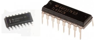
PWM controller TL494.
Let's figure out how the TL494 PWM controller works. It will be better if you download the datasheet www.ti.com/lit/ds/symlink/tl494.pdf, but in principle I will try to get the most important things out of it with the help of pictures. For a deeper understanding of all the subtleties, I recommend this document: www.ti.com/lit/an/slva001e/slva001e.pdf
Let's start, oddly enough, from the end - with the output part of the microcircuit. Now all attention is paid to the output of the OR element (marked with a red square). The output of this element at a specific point in time directly controls the state of one or both keys Q1 Q2. The control option is set via pin 13 (Output control).
Important thing No. 1: if the output of the OR element is log 1, the output keys are closed (turned off). This is true for both modes. Important thing No. 2: if the output of the OR element is log 0, one of the keys (or both at once) is open (enabled).
The following picture emerges: along the rising edge, the previously open transistor closes (at this moment they are both guaranteed to be closed), the trigger changes its state and, along the descending edge, another switch is turned on and will remain on until the rising edge comes again and closes it, at which time moment again the trigger clicks and the next descending edge will open another transistor. In single ended mode, the keys always work synchronously and the trigger is not used.
The time when the output is in the log. 1 (and both keys are closed) is called Dead time. The ratio of the pulse duration (log 0, transistor open) to the period of their repetition is called the duty cycle (PWM duty cycle). For example, if the coefficient is 100%, then the output of the OR element is always 0 and the transistor (or both) is always open.
Sorry, but I try to explain it as clearly as possible and almost on the fingers, because in official dry language it can be read in the datasheet.
Oh yes, why do we need Dead time? In short: in real life, the top key will pull up (toward the plus) and the bottom key down (to the minus). If you open them at the same time, there will be a short circuit. This is called through current and due to parasitic capacitances, inductances and other features, this mode occurs even if you open the keys strictly one by one. To minimize through current, dead time is needed.
Now let's turn our attention to the saw generator (oscillator), which uses pins 5 and 6 of the microcircuit to set the frequency. A resistor and capacitor are connected to these terminals. This is the same RC generator that many have probably heard about. Now at pin 5(CT) we have a saw from 0 to 3.3V. As you can see, this saw is fed to the inverting inputs of the Dead-time and PWM comparators.
We have more or less decided on the terms and operation of the output part of the PWM controller, now we will figure out what the saw has to do with it and why we need all these comparators and error amplifiers. We realized that the ratio of the pulse duration to the period of their repetition determines the duty cycle, and therefore the output voltage of the power source because The higher the fill factor, the more energy will be pumped into the primary winding of the transformer.
For example, let's figure out what needs to be done to set the fill factor to 50%. Do you still remember about the saw? It is supplied to the inverting inputs of the PWM and Dead time comparators. It is known that if the voltage at the inverting input is higher than at the non-inverting input, the comparator output will be log.0. Let me remind you that a saw is a signal that smoothly rises from 0 to 3.3V, after which it sharply drops to 0V. Thus, in order for the comparator output to be log.0 50% of the time, half of the saw voltage (3.3V/2=1.65V) must be applied to the non-inverting input. This will give the required 50% duty cycle.
We noticed that both comparators converge on the same OR element, which means that as long as one of the comparators produces log.1, the other cannot interfere with it. Those. The comparator that results in a lower duty cycle has priority. And if voltage is supplied to the Dead time comparator externally, then a signal can be supplied to the PWM comparator both externally (3 pins) and from the built-in error amplifiers (these are ordinary operational amplifiers). They are also connected using the OR circuit, but since... we are already dealing with an analog signal - the OR circuit is implemented using diodes. Thus, control over the duty cycle is taken over by the error amplifier that requests a smaller duty cycle. The condition of the other does not matter.
Feedback.
Okay, now how do you build a power supply around all this? Very simple! It is necessary to cover the power supply with negative feedback. The difference between the desired (specified) and available voltage is called an error. If at each moment of time we influence the duty cycle in such a way as to correct the error and bring it to 0, we obtain stabilization of the output voltage (or current). Feedback is negative as long as it reacts to an error with a control action of the opposite sign. If the feedback is positive, good luck! In this case, the feedback will increase the error instead of reducing it.
All this is work for those same error amplifiers. The reference voltage (reference) is supplied to the inverting input of the error amplifier, and the voltage at the output of the power supply is applied to the non-inverting input. By the way, inside the PWM controller there is a 5V reference voltage source, which is the reference point in all measurements.
Feedback Compensation
I don’t even know how to explain it in a simpler way. With feedback, everything is simple only in an ideal world. In practice, if you change the duty cycle, the output voltage does not change immediately, but with some delay.
For example, the error amplifier detected a decrease in voltage at the output, adjusted the duty cycle and stopped interfering with the system, but the voltage continues to increase and then the error amplifier is forced to adjust the duty cycle again in the other direction. This situation occurs due to a delayed reaction. This way the system can go into oscillation mode. They are damped and undamped. A power supply in which continuous oscillations of the feedback signal may occur will not last long and is unstable.
Feedback has a certain bandwidth. Let's assume a bandwidth of 100 kHz. This means that if the output voltage fluctuates with a frequency above 100 kHz, the feedback simply will not notice this and will not correct anything. Of course, I would like the feedback to respond to changes in any frequency and the output voltage to be as stable as possible. Those. The struggle is to ensure that feedback is as broad as possible. However, this same reaction delay will not allow us to make the band infinitely wide. And if the bandwidth of the feedback circuit is wider than the capabilities of the power supply unit itself for processing control signals (direct connection) - at some frequencies the negative feedback will suddenly become positive and, instead of compensating for the error, it will increase it even more, and these are precisely the conditions for the occurrence of oscillations.
Now from delays in seconds, let's move on to frequencies, gains and phase shifts... Bandwidth is the maximum frequency at which the gain is greater than 1. As the frequency increases, the gain decreases. In principle, this is true for any amplifier. So, for our power supply to work stably, one condition must be met: in the entire frequency band, where the total gain of forward and feedback is greater than 1 (0 dB), the phase lag should not exceed 310 degrees. 180 degrees introduces the inverting input of the error amplifier.
By introducing various filters into the feedback loop, we ensure that this rule is followed. Very roughly speaking, feedback compensation is adjusting the bandwidth and phase response of the feedback to the reactions of the real power source (to the characteristics of the feedforward connection).
This topic is not very simple, there is a lot of mathematics, research and other works under it... I’m just trying to present the very essence of the issue in an accessible way. I can recommend reading this article, where, although not very clear, this issue is also covered in an accessible form and links to literature are given: bsvi.ru/kompensaciya-obratnoj-svyazi-v-impulsnyx-istochnikax-pitaniya-chast- 1
From theory to practice
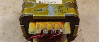
Now we can look at the power supply diagram and understand that there is a lot of unnecessary stuff in it. First of all, I unsoldered everything related to monitoring the output voltages (Power good signal generation circuit). I neutralized the error amplifiers built into the PWM controller by applying +5vref to the inverting inputs and setting the non-inverting inputs to GND. Removed the standard short circuit protection circuit. I cut out all the unnecessary output filters from voltages that are not used... Replaced the output diodes with more powerful ones. Replaced the transformer! I unsoldered it from a high-quality power supply where the written 400W really means 400W. The difference in size between what stood here before speaks for itself:
I replaced the chokes in the output filter (from the same 400W power supply) and set the capacitors to 25V:
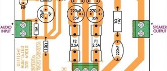
Next, I developed a circuit that allows you to regulate the stabilization of the output voltage and set a limit on the current output from the power supply.
The circuit implements external error amplifiers assembled on operational amplifiers LM358 and several additional functions in the form of a shunt amplifier (INA197) for measuring current, several buffer amplifiers for outputting the value of the set and measured current and voltage to another board where the digital indication is assembled. I will talk about it in the next article. Providing signals as they are to another board is not the best solution because... the signal source may be quite high-impedance, the wire picks up noise, preventing the feedback from working stably. In the first iteration I encountered this and had to redo everything. In principle, everything is signed on the diagram; I see no point in commenting on it in detail and I think that for those who understand the theory above, everything should be quite obvious.
I will only note that the C4R10 and C7R8 chains are the feedback compensation that I spoke about above. To be honest, the excellent article by the embadder under the nickname BSVi helped a lot in setting it up. bsvi.ru/kompensaciya-obratnoj-svyazi-prakticheskij-podxod This approach really works and after spending a day or two I managed to achieve stable operation of the power supply using the method described in the article. Now, of course, I could have done it in probably two hours, but then I had no experience and through negligence I blew up quite a few transistors.
Oh yeah, check out the C7 capacity! 1uF is quite a lot. This was done in order to tighten the current feedback in speed. This is such a dirty hack to overcome the instability that occurs at the border of the transition from voltage stabilization to current stabilization. In such cases, they use some more sophisticated techniques, but I didn’t bother like that. I don’t need super accurate current stabilization, and besides, by the time I encountered this problem, I was really tired of the project of remaking the power supply!
According to this scheme, a board was made using a laser iron:
It is built into the power supply like this:
A piece of copper wire, probably 10 centimeters long, was chosen as a shunt for measuring current.
I used the case from a fairly high-quality Hiper power supply unit. This seems to be the most ventilated building I've ever seen.
There was also a question about connecting the fan. The power supply is adjustable from 0 to 24V, which means the cooler will have to be powered from the control room. The control room is represented by two voltages - stable 5V, which goes to the motherboard and unstabilized, service power of about 13.5V, which is used to power the PWM controller itself and to drive the control transformer. I used a regular linear stabilizer to get stable +12V and connected it to a small cooler speed thermoregulation board soldered from the same Hiper. I secured the scarf to the radiator with a screw simply for the convenience of connecting the cooler.
By the way, the radiators had to be bent because they did not fit into the body of the new format. It is better to heat them with a soldering station before bending, otherwise there is a chance of breaking off half of the teeth. The regulator thermistor was attached to the group stabilization throttle because this is the hottest part.
In this form, the power supply went through long-term tests, powering a bunch of car high-beam light bulbs and withstanding current loads of about 20A at a voltage of 14V. He also proudly charged several car batteries when the lights were turned off in Crimea.
The future is already here
In the meantime, I came up with a slightly non-standard system for indicating power supply operating modes, which I later regretted a little, but it still works!
So in the next article you will find programming ATMega8 in C++ using template magic, various patterns and a self-written library for fixed-point calculations on top of which averaging of ADC samples is implemented and converting them into voltage/current using a table with linear interpolation. By some miracle, all this fit into 5 and a few kilobytes of flash.
Don't change the channel, it should be interesting.
By the way, the book promised at the beginning: Kulichkov A.V. “Switching power supplies for IBM PC” radioportal-pro.ru/_ld/0/15_caf3ebe8f7eaeee.djvu
PS I hope the above will be useful. Don't judge strictly, but constructive criticism is welcome.
Added for RO users who cannot write comments:
email: altersoft_dog_mail.ru
So, ATX has risen.
The frequency of the internal oscillator is determined by the formula:
Pin 14 is the output of the internal +5 volt reference voltage.
Pins 1,2,15 and 16 are the inputs of 2 built-in comparators, which the user can use at his discretion, i.e. control the width of the PWM output pulses. Both comparators are exactly the same, with the only difference being that the comparator with pins 15-16 operates with a “delay” of 80 mV. In the ATXs I received, this comparator was not used, pin 16 is grounded, and pin 15 is connected to Uref, i.e. 14 output.
Pin 13 is intended for switching the TL-494 into control mode for flyback single-ended converters. In this case, the “dead time” can be increased to 96%. In our “push-pull” case, this pin is also connected to Uref.
We will use the comparator on pins 1-2 to set the output voltage; for this, we apply part of Uref to pin 2, which is done in most AT and ATX. Typically this voltage is approximately 2.5 volts, i.e. with Uref (+5Volt) through a resistive divider.
The RC chain from pin 2 to pin 3 (FB or OS) is designed to limit the PWM speed while stabilizing the voltage and is available in all AT-ATX circuits. It also cannot be cut out.
I am drawing a simplified output voltage control circuit.
The principle of operation of the microcircuit
The PWM controller has a fairly simple operating scheme. With a standard connection, control signals begin to flow under incoming voltage to the inputs of the microcircuit. If the power is below 3 V, then pulses are formed at the output, and their width varies depending on the connection characteristics.
The circuits are used only in the case of high forward signals. The voltage level is regulated at the outputs, which can control it at the output streams.
Attention! The main operating principle of the installation largely depends on the control signal. It causes a linear drop or rise in voltage internally. Pulses of various types can be used as signals. One of the methods to study the operating features of the circuit is to use an oscilloscope by connecting it to the points of the test board.
Settings
Let's launch. We're blown away by the amount of noise!
300mV! Packs seem to be arousing feedback. We slow down the OS to the limit, the packs do not disappear. So it's not an issue with the OS.
After poking around for a long time, I found that the cause of the noise was the wire! O_o A simple two-core two-meter wire! If you connect an oscilloscope before it, or connect a capacitor directly to the oscilloscope probe, the ripple is reduced to 20 mV! I can’t really explain this phenomenon. Maybe some of you can share? Now, it’s clear what to do - there must be a capacitor in the power supply circuit, and the capacitor must be hung directly on the power supply terminals.
By the way, about Y - capacitors. The Chinese saved on them and did not supply them. So, the output voltage without Y-capacitors
And now - with the Y capacitor:
Better? Without a doubt! Moreover, after installing the Y-capacitors, the current meter immediately stopped glitching!
I also installed X2 – a capacitor, so that there would be at least less rubbish in the network. Unfortunately, I don’t have a similar common-mode choke, but as soon as I find it, I’ll install it right away.
Feedback.
I wrote a separate article about her, read
Cooling
This is where we had to tinker! After a few seconds under full load, the question of the need for active cooling was removed. The output diode assembly heated up the most.
The assembly contains ordinary diodes, I was thinking of replacing them with Schottky diodes. But the reverse voltage on these diodes turned out to be about 100 volts, and as you know, high-voltage Schottky diodes are not much better than conventional diodes.
Therefore, we had to attach a bunch of additional radiators (as many as we could fit) and organize active cooling.
Where to get power for the fan? So I thought for a long time, but finally came up with it. tl494 is powered by a 25V source. We take it (from jumper J3 in the diagram) and lower it with the 7812 stabilizer.
For ventilation, I had to cut out a cover for a 120mm fan, attach a corresponding grille, and set the fan itself to 80mm. The only place where this could be done was the top cover, and therefore the design turned out to be very bad - some kind of metal crap could fall from the top and short-circuit the internal circuits of the power supply. I give myself 2 points. You shouldn't have left the power supply housing! Don't repeat my mistakes!
The fan is not attached in any way. The top cover just presses it down. So I got the size right.
results
Bottom line. So, this power supply has been working for a week now and we can say that it is quite reliable. To my surprise, it emits very little, which is good!
I tried to describe the pitfalls that I ran into. I hope you don't repeat them! Good luck!
Good afternoon. I would like to clarify the values of resistors R3, R8, R14 and R18, the parameters L1 in the control electronics, the values of resistors R22 and R25 in the false panel, and whether it is possible to lay out printed circuit boards. Thank you.
Of course, respect to the author for the development! But to repeat it, you must first disenchant the power supply control circuit, which is in the PDF. Crap! What makes you encrypt the scheme first? And the one for whom it is posted here then deciphers this scheme. What kind of moron came up with this idea? Was it really impossible to properly draw both control schemes (pdf) on one sheet and without any links like: Vref, AGND... What kind of mediocrity is this. BSVi - a big disadvantage for you in drawing diagrams! You are mediocrity. Never do this again. Ask the experts to do it
The author did a decent job and wrote a useful article. As for the diagrams, excuse me, on the contrary, you are showing your ignorance