Many people are familiar with the situation when some device plays sound, but does not do it as loudly as we would like. What to do? You can buy other sound-reproducing equipment, or you can buy an audio frequency power amplifier (hereinafter referred to as UMZCH). Moreover, the amplifier can be assembled with your own hands.
To do this, you will only need basic knowledge of electronics, such as the ability to distinguish between the emitter, base and collector in a bipolar transistor, drain, source, gate in a field effect transistor, as well as other elementary aspects.
Next, we will describe the most important parameters of audio power amplifiers, which are worth working on to improve in order to achieve greater gain, as well as the simplest circuits of these devices, assembled on various basic components such as vacuum tubes, transistors, operational amplifiers and integrated circuits.
In addition, the article will consider a scheme for a high-quality UMZCH. Its composition, parameters, as well as design features will be affected. The Sukhov UMZCH circuit will also be considered.
UMZCH parameters
The most important parameter of a power amplifier is the gain. It represents the ratio of the output signal to the input signal and is divided into three separate parameters:
- Current gain. KI = Iout / Iin.
- Voltage gain. KU = Uout / Uin.
- Power gain. KP = Pout / Pin.
In the case of UMZCH, it is more reasonable to consider the power gain, since it is this parameter that is required to be amplified, although it is foolish to deny that the amount of power - both input and output - depends on the magnitudes of current and voltage.
Of course, amplifiers have other parameters, such as the distortion factor of the amplified signal, but all of them are not so important compared to the gain factors.
Do not forget that there are no ideal devices. There is no UMZCH with a huge gain, devoid of other disadvantages. You always have to sacrifice some parameters for the sake of others.
UMZCH on electric vacuum devices
Electrovacuum devices are devices that contain in their design a flask containing either a vacuum or a certain gas, as well as at least two electrodes - a cathode and an anode.
Inside the flask there can be three, five, or even eight additional electrodes. A lamp with two electrodes is called a diode (not to be confused with a semiconductor diode), with three - a triode, with five - a pentode.
Power amplifiers based on vacuum tubes are very highly valued both among ordinary music lovers and among professional musicians, because the tubes provide the “cleanest” amplification.
This is partly due to the fact that electrons injected from the cathode do not encounter resistance on their way to the anode and reach the target in an unchanged state - they are not modulated in either density or speed.
Tube amplifiers are the most expensive of all those on the market. This is due to the fact that electric vacuum devices ceased to be widely used in the last century, and accordingly, their production in large quantities became unprofitable. This is a piece product. But such UMZCHs are definitely worth the money: in comparison with popular analogues, even on integrated circuits the difference is clearly audible. And not in favor of microcircuits.
Of course, it is not necessary to assemble tube amplifiers yourself; you can purchase them in specialized stores. The cost of amplifiers using electric vacuum devices starts from ₽50,000. You can find relatively cheap used options (even up to ₽10,000), but they may be of poor quality. How much do good tube amplifiers cost? From ₽100,000. How much do very good amplifiers cost? From several hundred thousand rubles.
There are many UMZCH circuits based on lamps; in this section we will consider an elementary example.
The simplest amplifier can be assembled using a triode. It belongs to the class of single-cycle UMZCH circuits. In a triode, the third electrode is the control grid, which regulates the anode current. An alternating voltage is connected to it and using the magnitude and polarity of the source signal, you can either decrease or increase the anode current.
If you connect a negative high potential to the grid, then electrons will settle on it and the current in the circuit will be zero. If a positive potential is applied to the grid, then electrons from the cathode to the anode will pass unhindered.
By adjusting the anode current, you can change the operating point of the triode on the current-voltage characteristic. This allows you to adjust the amount of current and voltage amplification (and ultimately power) of this vacuum device.
To assemble a simple triode amplifier, you need to connect an alternating power source to the control grid, apply zero potential to the cathode, and positive potential to the anode. A ballast resistor is usually connected to the anode. The load should be removed between the ballast and the anode.
To improve the quality of the amplified signal, you can connect a filter capacitor in series or in parallel (depending on the specific case) to the load, connect a parallel-connected capacitor and resistor to the cathode, and connect a simple voltage divider of two resistors to the control grid.
Theoretically, a power amplifier can be assembled on a klystron using UMZCH circuits on lamps. A klystron is an electric vacuum device similar in design to a diode, but has two additional terminals that serve as signal input and output. Amplification in this device occurs by modulating the flow of electrons emitted by the cathode towards the collector (analogous to the anode), first in speed and then in density.
Quality and circuitry of UMZCH
Manufacturing a high-quality UMZCH is not yet a solution to the problem, since it is only one of the links in the chain of devices that form a sound-reproducing complex. And such a complex should be created systematically, starting with the development of requirements based both on the desired results and on the available capabilities. In this case, not only the technical characteristics of the sound reproduction path should be taken into account, but also the parameters of the loudspeakers, the acoustic parameters of the room, issues of ergonomics and reliability. Many of these requirements are mutually contradictory, so the solution to such a problem can only be achieved by a large team of designers, united by a common idea, such as the army of radio amateurs.
I would like to continue developing ideas that contribute to achieving high results in the manufacture of high-quality complexes of varying degrees of complexity. And start not with their electrical characteristics, but with their composition and design.
According to the author, the radio complex, in addition to the amplification-switching device, should include an electronic control unit, a cassette recorder-attachment and a tuner with the main parameters that provide a total effect corresponding to the acoustic characteristics of the loudspeakers. The complex may also include a reel-to-reel tape recorder with higher parameters than other units for dubbing programs from cassettes and reels. Structurally, the named parts of the radio complex must be combined into an indivisible music center. The existing opinion about the possible further development of the radio complex, the blocks of which are interconnected by numerous cables, is not shared by the author. The fact is that with consistent characteristics of the blocks providing a given quality of audio reproduction, improving the parameters of one of them will not lead to an improvement in the overall effect. The latter can only be obtained if the radio complex consists of elements with different, obviously worse quality parameters, and this is fundamentally wrong. But even if such a radio complex satisfies the sound of its owner when working with loudspeakers of a low complexity group, then it will immediately cease to satisfy him after replacing them with an acoustic system of a higher group: the shortcomings of the weak links will immediately begin to appear.
Thus, when replacing loudspeakers, the need to replace other units inevitably arises, and if their characteristics are consistent, the entire radio complex. That is why it is advisable to perform it in the form of blocks combined into a musical center, coordinated according to the main parameters. This design of the complex ensures increased reliability, improved quality and ergonomic characteristics. The gain in reliability is determined by the absence of connecting cables and the impossibility of incorrect connections, in technical characteristics - by facilitating the fight against background noise, in ergonomics - by the possibility of expedient placement of controls and the components themselves when arranging the music center as a whole.
Thesis: loudspeakers are the most important component of a radio complex and hardly require any special explanation. We can talk about the quality of any link in the sound reproduction path, about the influence of its parameters on the quality of sound reproduction, but if an electroacoustic converter cannot convert electrical signals into sound signals in a certain frequency range with an acceptable level of distortion, then, as a rule, no improvement in other nodes of the path will lead to to a proportional improvement in sound. Of course, the degree of speaker damping by the output impedance of the UMZCH can to some extent affect the quality of playback, but only until it reaches the limiting value for a given electroacoustic transducer. By frequency correction of the amplifier, you can expand the range of frequencies reproduced by the speaker system, but to the detriment of another parameter - the dynamic range of signals amplified without nonlinear distortion.
Loudspeakers have to be selected not only according to parameters and cost, but also taking into account the possibility of their placement in a residential area, where they, apparently, should not be the main element of the interior. The last circumstance is often decisive: not every family would risk making the main decoration of their apartment two bulky and not always elegantly designed loudspeakers.
To bridge the gap between the desired quality of sound reproduction and the possibilities of placing loudspeakers in an apartment, the main efforts of industry and amateur radio designers should apparently be directed towards creating sufficiently high-quality, small-sized, aesthetically competently designed and affordable speaker systems. Their frequency range, according to the author, should be no more than 30...16,000 Hz. Its further expansion for household radio equipment is hardly advisable. The harmonic distortion factor in the specified frequency range should not exceed 3% at a rated power of 25 W.
Almost the same requirements for frequency characteristics should be presented to the second most important link of the radio complex - UMZCH: the optimal frequency range for its length can be considered 20-20000 Hz (with a drop in frequency response at the edges of no more than - 3 dB). The harmonic coefficient, which could well reach 0.5-1%, would not be fundamental if the nonlinearity of the amplitude characteristic of the UMZCH did not lead to the appearance of non-harmonic components in the spectrum of the amplified signal, called nitromodulation distortions. It is they, and not the harmonic components, that are the source of unpleasant overtones. Frequency components lying beyond the upper limit of the sound range and, therefore, not audible by the ear, when located close to them on the frequency axis, can generate combination frequencies that fall within the region of maximum sensitivity of the human ear [6]. The high slope of the characteristics of bipolar transistors, and therefore the curvature (nonlinearity) lead to the appearance of combinational components of a fairly high (6th - 10th) order with significant levels.
The fight against intermodulation distortion that occurs when the signal is limited is quite simple: it is enough to correctly select the voltage amplitude at the input of the UMZCH.
The crest factor of a multi-frequency signal is close to the crest factor of noise and is most likely equal to 3. Therefore, the input voltage for undistorted sound reproduction should be 3 times less than the maximum value at which the output sinusoidal signal is not yet distorted. The required input voltage level is selected by setting the volume control to the position corresponding to the maximum volume. It should, however, be taken into account that the average output power will be approximately equal to 0.1 of the nominal power, and the sound volume for the selected acoustic system and a specific room will be determined by it. Considering that the most typical volume of a living space, which is 40-60 m3, requires an average power of about 4 W, the nominal total power of a stereo UMZCH should be 40 W - 20 W per channel. This value should, in the author’s opinion, be considered the minimum for high-quality sound reproduction.
Obviously, at the specified output power, intermodulation distortion should be below the noise level of the UMZCH. However, measuring intermodulation distortion at a level of -70 dB (0.03%) in the presence of a high-level main signal can only be done with a spectrum analyzer with a dynamic range of at least 80 dB. Unfortunately, such devices are practically inaccessible to most radio amateurs. Indirectly, the magnitude of intermodulation distortion can be judged by the harmonic distortion coefficient, but there is also practically nothing to measure this parameter at the level of -70 dB: there is no suitable nonlinear distortion meter available to a radio amateur.
True, there is a well-known method of mutual compensation of the input and output signals of the UMZCH. Estimating distortion in this way is most acceptable for radio amateurs, however, at levels of -70 dB, certain difficulties arise in this case. Therefore, the primary task of radio amateur designers, in the author’s opinion, should be the development of intermodulometers that can be replicated. And until they appear, you will have to use less objective, but more accessible methods.
The examination method gives good results and is accessible to a wide range of radio amateurs. The observations of Yu. Solntsev are in good agreement with the observations of the author. Some of the conclusions from them are worth repeating, giving them the meaning of quality assessment criteria. This is, firstly, achieving the best sound of high-quality phonograms when setting the frequency response controls of the preamplifier to the middle position. Any desire to give the frequency response a form other than linear, especially in the higher frequencies, always indicates the nonlinearity of the amplitude characteristics of the UMZCH, leading to the appearance of intermodulation and harmonic components in the spectrum of the output signal.
Secondly, testing the amplifier with a signal of the same musical content, but with harmonic distortion introduced into it, for example, when recording on a tape recorder of relatively low quality. The more linear the UMZCH, the less the apparent difference from the original will be. The presence of harmonic components in the spectrum of the phonogram, which do not yet significantly reduce the quality when playing through an UMZCH with a linear amplitude characteristic, leads to intermodulation distortion and non-harmonic clogging of the output signal when listening through an amplifier with an insufficiently linear characteristic, which is immediately detected even by not very experienced ears.
Objective methods for assessing the quality of UMZCH, as well as any radio-electronic device, should include the examination of circuit solutions. Of course, such an assessment requires certain knowledge in the field of radio electronics and is beyond the capabilities of radio listeners without radio engineering training, but it is quite accessible to radio amateurs who are able to compare the circuitry features of a particular amplifier using the method proposed below.
First of all, you should pay attention to the output stage of the UMZCH. It is known that it is very difficult to achieve an acceptable level of nonlinear distortion in amplifiers operating in mode B at low output power.
It is also known that mode A in UMZCH leads to an unacceptable decrease in efficiency and significant design costs for heat removal from the output transistors.
The intermediate AB mode is also not without its drawbacks: it requires careful selection of the mode of the output stage transistors and temperature stabilization of their quiescent current. The use of various thermal environmental protection systems is structurally complex and inertia is unacceptable. The current collectors of trimming resistors, with the help of which the quiescent current of the output transistors are set, oxidize over time and can cause the transistors of the final stage to fail.
The most successful solution, according to the author, is a combination of amplifiers operating in modes A and B (and even A and C), and one in which only the first of them works at low output power, and both at high power (low-power amplifier , operating in mode A, is simultaneously the exciter of the output stage, the transistors of which operate in mode B and are closed at low signal levels). This makes it possible to abandon the stabilization of the operating point of the transistors of the final stage, ensuring the constancy of the mode of only the low-power amplifier. The OOS in such amplifiers operates in both small and large signal modes, which is achieved by direct coupling of the input and output of the final stage.
To increase the linearity of the amplitude characteristics of preamplifiers, the supply voltage must significantly (5-10 times) exceed the amplitude of the required output voltage. This is especially important for amplification stages of tone blocks and equalizers, in which linear amplification must be ensured with a maximum increase in the frequency response in the corresponding areas of the audio frequency range.
For the same purpose, preamplifiers should be made on the basis of differential stages in combination with emitter followers. The advantage of the former is significantly greater linearity compared to the OE cascade (to obtain a harmonic distortion equal to 1%, it is enough to apply a voltage of 1 mV to the input of the OE cascade, while the differential cascade introduces such distortion at a level 18 times higher), the latter - 100%. - low current feedback, correcting distortion, and low output impedance, reducing interference.
The distribution of gain along the path of the radio complex is very significant. On the one hand, the nominal input voltage of the UMZCH must guarantee the absence of background interference and a significant excess of signal over noise (the same 70 dB), on the other hand, it should not lead to signal distortion in the preamplifiers due to the peaks of the complex signal entering the limiting region .
The most correct thing would be to choose the sensitivity of the UMZCH as high as possible (in excess of noise), and to combat background interference with circuitry and design solutions. One of them would be, for example, the use of a symmetrical input stage of the UMZCH with the conclusion of both wires coming to it from the preamplifier into a common screen and the connection of this screen and one of the signal wires with a common wire on the preamplifier board. Purely constructive solutions include combining the radio complex units into a music center, where they are all powered by one network transformer; rational placement of components (primarily the network transformer, EPU motors and tape recorder) in relation to one another, inputs, amplifiers, switching devices, volume and tone controls; correct implementation of shielding and common wire bus.
According to the author, it is advisable to reduce the nominal input voltage of the UMZCH and set it to 0.25 V.
All of the mentioned circuitry conditions for ensuring high quality of the amplification part of the radio complex, at first glance, require its significant complication. However, the use of op-amps in all links of the path makes it possible to achieve the desired results with ease of implementation.
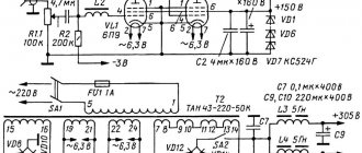
Rice. 1
The schematic diagram of this amplifier (using domestic parts) is shown in Fig. 1. Its first stage is made on op-amp DA1, connected together with transistors VT1 and VT2 in such a way as, firstly, to increase the rate of voltage rise at the amplifier output, and secondly, to provide the nominal supply voltage of the op-amp. The pre-terminal stage (VT3 and VT4) operates in mode A, the output stage (VT5 and VT6) - in mode B. Diodes VD1 and VD2 guarantee the absence of quiescent current in the output stage when the current through transistors VT3 and VT4 changes (due to their heating) by 1, 5-2 times. The purpose of the OOS, common for direct and alternating currents, does not contain a large capacitor and has a small time constant for transient processes. Elements R10, R11 C5 and L1 correct the phase response of the OOS circuit, ensuring, when properly configured, a low level of intermodulation distortion and harmonic distortion. The parameters of these elements are related by a simple relationship (L1 = R10R11C5) and can be easily calculated for each specific case.
With a supply voltage of ±30 V, a load resistance of 4 Ohms and an input voltage of 100 mV, the UMZCH produces a maximum power of 100 W. With a rated power of 60 W, the harmonic distortion coefficient at a frequency of 1000 Hz does not exceed 0.006%.
The author tested this UMZCH with a supply voltage of ±20 V and a load resistance of 4 Ohms (the values of the elements R5, R6, C5, R11 were changed). The nominal input voltage was chosen to be 0.75 V (if desired, it can be changed in any direction by selecting resistor R3). The setup came down to setting the quiescent current of transistors VT3 and VT4 (within 10-20 mA) by selecting resistors R7 and R8 in the absence of current through transistors VT5 and VT6. When powered from a stabilized source, the UMZCH in the frequency range 20-20000 Hz provided a maximum output power of 40 W, and from an unstabilized source - about 35 W. The harmonic distortion coefficient at a frequency of 1000 Hz with an output power of 20 W, measured by a vector harmonic distortion indicator, did not exceed 0.01%. The tests were carried out jointly with I. T. Akulinichev. Subjectively, the amplifier provides higher quality sound reproduction than a musical UMZCH, satisfying the evaluation criteria. The results obtained confirmed the possibility of creating a high-quality UMZCH that is simple in circuit design.
Rice. 2
A possible version of the printed circuit board is shown in Fig. 2. It is designed for the installation of MLT resistors and KM capacitors (the purpose of the elements shown in dashed lines will be discussed below). Coil L1 is wound in two layers (9+7 turns) with PEV-2, 0.8 wire on a mandrel with a diameter of 7 mm and is impregnated with Moment-1 glue for rigidity.
The described UMZCH does not have protection against short circuits in the load and does not contain devices that protect loudspeakers in the event of a breakdown of one of its transistors. According to the author, these functions are quite capable of being performed by calibrated fuses.
The circuit solutions used in the amplifier ensure that there are no clicks in the speakers when the power is turned on and off.
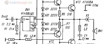
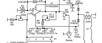
Rice. 3
When used in conjunction with an UMZCH pre-amplifier, which has a constant voltage at the output, clicks may appear due to its fault. In this case, you can use an acoustic system protection device made according to the diagram in Fig. 3. It is triggered when a voltage of more than 1.2 V of any polarity appears at the output of the UMZCH, including if the voltages at the channel outputs have different polarities. Speaker connection delay is 1.5-2 s. The use of zener diodes VD5 and VD6 with a low stabilization voltage protects op-amp DA1 from input overloads at significant levels of constant voltage at the outputs of the stereo amplifier channels. To power the device, a separate winding of a network transformer with a voltage of 5-6 V is required.
To obtain zero potential at the output of the rumble filter, it is necessary to apply additional bias from a positive voltage source to the base of transistors V1 and V1′ through resistors with a resistance of 68-82 kOhm.
In conclusion, a few words about the choice of parts. The parameters of the amplification path largely depend on the element base. In particular, op-amps that are supposed to be used in preliminary or correction amplifiers should not contain transistors operating in mode B in the output stage, as is the case, for example, in the K153UD1. Op-amps intended for UMZCH, similar to the circuit shown in Fig. 1, must necessarily have a push-pull output stage operating in AB mode (K140UD6, K154UD1, K154UD2, K154UDZ, K140UD7, K544UD2, etc.). In addition, it is advisable to use an op-amp with an output voltage slew rate of at least 2 V/µs.
Some of these op amps require balancing or the inclusion of a correction circuit. In this case, the printed circuit board (Fig. 2) has holes for installing balancing resistors R15, RI6 (their total resistance is about 10 kOhm) and correction capacitor C13. The printed conductor, to which the terminals of resistors R15, R16 are soldered, is connected to the corresponding power supply terminal of the op-amp. When using op-amps K544UD2, K154UD1—U154UDZ at the UMZCH input, it is recommended to turn on the low-pass filter. consisting of resistor R14 (10 kOhm) and capacitor C12 (150 pF).
In amplifiers with. With input and output potentials close to 0, oxide capacitors, including non-polar ones, cannot be used as transition capacitors. All oxide capacitors require a polarizing voltage of 410 times the amplitude of the applied AC voltage. Failure to do this reduces the reliability of the amplifier and may lead to additional distortion.
All transistors through which the signal passes in the amplifier path must be high-frequency, and those used in the input stages must be low-noise. In power amplifiers, it is desirable to use transistors with a metal case, since it is very difficult to ensure good heat dissipation with the existing design of metal-plastic cases.
Used Books:
- Lexina Valentin and Victor. On the visibility of nonlinear distortions of a power amplifier. - Radio, 1984, No. 2, p. 33-35.
- Solntsev Yu, High-quality power amplifier. - Radio, 1984, No. 5, p. 29—34
- Solntsev Yu. What Kg is acceptable? —Radio, 1985, No. 2, p. 26-28.
- Ataev D.. Bolotnikov V. How to reduce the level of interference in the AF path. - Radio, 1984, No. 4, p. 43-45; No. 5, p. 35, 36.
- Ataev D., Bolotnikov V. Unification in amateur radio designs. - Radio, 1983, No. 12, p. 32-35.
- Pickersgnl A., Bespalov I. The phenomenon of “transistor” sound. - Radio, 1981, No. 12, p. 36-38.
- Efimov A., Efimov B., Thomas G. Selecting the power of stereo amplifiers. - Radio, 1977, No. 6, p. 39-41.
- Akuliinchev I. Selection of distortion signal. - Radio. 1983, No. 10, p. 42-44.
- Tntze U., Schenk K. Semiconductor circuitry. - M.: Mir, 1982.
- Schmidt G. Current dumping amplifier.— Elector. 1978, No. 7/8.
- Roganov V. Loudspeaker protection device. - Radio, 1981. No. 11, p. 44. 45.
- Ageev A. Amplifier block of an amateur radio complex. - Radio, 1982, No. 8, p. 31-35.
- Solntsev Yu. High-quality pre-amplifier. - Radio, 1985, No. 4, p. 32-35.
- Lexina Valentin and Victor. Preamplifier-corrector with rumble filter, - Radio. 1983, no. 7, p. 48-50.
Author: Gumelya E.
From the magazine “Radio” No. 9, 1985.
UMZCH on bipolar transistors
Bipolar transistor - synthesis of two diodes. It is either a pnp or npn element having the following components:
- emitter;
- base;
- collector.
The speed and reliability of transistors is generally higher than that of electric vacuum devices. It's no secret that at first electronic computers worked on tubes, but as soon as transistors appeared, the latter quickly replaced their antediluvian competitors and are successfully used to this day.
Next, we will consider an example of using an NPN transistor in a power amplifier circuit. It is important to note that electrons (n) are slightly faster than holes (p); accordingly, the performance of npn and pnp transistors differs not in favor of the latter.
Another important nuance is that bipolar transistors have several switching schemes:
- With a common emitter (the most popular).
- With a common base.
- With a common collector.
All circuits have different gain parameters. The following UMZCH circuit has a connection with a common emitter.
To assemble a simple amplifier using an NPN transistor, you need to connect an alternating voltage to its base, a positive potential to the collector, and a negative potential to the emitter. Limiting resistances should be installed in front of the base, in front of the collector, and in front of the emitter. The load is removed between the collector ballast resistance and the collector itself.
As in the case of a triode vacuum amplifier, to improve the quality of amplification in this circuit you can:
- install a voltage divider and filter capacitor in front of the base;
- install a parallel-connected capacitor and resistor on the emitter;
- turn on a filter capacitor to the load to eliminate noise and interference.
If two such amplifier stages are connected in series, their gains can be multiplied by each other. This, of course, will significantly complicate the design of the device, but will allow for greater gain. True, it will not be possible to endlessly connect these cascades: the more single amplifiers are connected in series, the greater the chance that they will go into saturation.
If the transistor operates in saturation mode, then there can be no talk of any amplifying properties. You can verify this by looking at the current-voltage characteristic: the operating point of the transistor is in the horizontal section if it operates in saturation mode.
The simplest high-quality UMZCH in a computer (part 1)
For comfortable listening to audio content, it is necessary to ensure a sufficient sound pressure level at the listening location. Thus, when watching television at home, the root mean square sound pressure level is 60 dB [1]. Exceeding this level too much can be harmful to health. We will limit the average sound pressure level to a health-safe value of 70 dB [1]. And let’s take a margin of 18 dB for undistorted reproduction of signal peaks [2].
Then the UMZCH of a computer acoustic system (AS) will require an output power that provides a sound pressure of 88 dB at signal peaks. This corresponds to an rms sine wave of 85 dB (3 dB below peak level).
Let bookshelf speakers with an impedance of 4 Ohms and a characteristic sensitivity of 90 dB be used with a personal computer (PC). When a sinusoidal signal with a voltage of 2 V is applied to such a speaker at a distance of 1 m, a sound pressure of 90 dB will be created, corresponding to the characteristic sensitivity. A stereo pair of such speakers will create a sound pressure of 93 dB [3, p. 116]. And to achieve a sound pressure of 85 dB on a sinusoidal signal, it is enough to supply each speaker with a signal with an effective voltage value not of 2 V, but 93 - 85 = 8 dB less, i.e. 0.8 V or 160 mW in power.
An output voltage of 0.8 V is provided by many digital-to-analog converters (DACs) of built-in PC sound cards. In this case, in order to provide the power necessary for comfortable listening in accordance with the above estimates, the UMZCH only needs to amplify the current. An emitter follower (cascade with a common collector) copes with this task. The traditional emitter follower circuit contains a resistor in the emitter circuit, the signal from which is supplied to the load through a decoupling capacitor. A resistor connected to the emitter circuit dissipates part of the signal power. These losses can be avoided by connecting the load directly to the emitter circuit, which is implemented in the proposed UMZCH. This solution not only simplifies the UMZCH, but also improves its quality due to the reduction in the length of the sound reproduction path.
Rice. 1. Diagram of one UMZCH channel
The diagram of one channel of the proposed UMZCH is shown in Fig. 1. There is no input coupling capacitor here, since such a capacitor is present at the DAC output of the PC sound card. The signal to the UMZCH input can be supplied either from a linear output located on the rear panel of the PC, or from a connector on the motherboard designed to connect to the microphone and telephone connectors on the front panel of the PC system unit. The 5 V supply voltage can be taken from the internal Molex connector of the PC system unit.
The 2SC3807 transistor with a supply voltage of 5 V and a load resistance of 4 Ohms has a minimum harmonic distortion coefficient (THD) with an emitter current of about 0.5 A. In this case, a power of 1 W is supplied to the speakers with a resistance of 4 Ohms, which is significantly less than the rated power of many bookshelf speakers .
In addition to the 2SC3807 transistor, other transistors were tested in the amplifier: KSD1273, KSC1983, 2SD1829, CEP603AL, KT819V, KT972A, GT404B. However, the 2SC3807 transistor showed the best results.
The UMZCH does not require a separate power supply, which greatly simplifies its design. A low supply voltage helps protect transistors in the event of a short circuit in the load and protect the AC in the event of a transistor breakdown. Each channel of the UMZCH can be powered from a separate port of the USB-2 connector of the PC motherboard, since this port provides a load current of up to 0.5 A. The common wire for the UMZCH should be connected to one point. For example, if the common wire is connected to a Molex connector or to a USB connector pin, the cable shield from the linear output of the PC should not be connected on the UMZCH side. UMZCH transistors are installed on a heat sink and placed in a convenient place inside the PC case. Only wires for connecting speakers are removed from the housing.
Despite its simplicity, the proposed UMZCH has the characteristics of amplifiers that meet High End criteria:
— operation of transistors in class A;
— absence of any feedback on the amplified current;
- the amplification path has the minimum possible length, since it contains a single element - a transistor.
Measurements of the parameters of this UMZCH were carried out using a sound card built into the motherboard on the ALC892 chip [4]. Some typical parameters of this microcircuit: DAC output voltage - 1.2 V; dynamic range of analog-to-digital converter (ADC) - 92 dB; DAC dynamic range - 97 dB; output impedance - 200 Ohm. The measured parameters of the sound card are given in table. 1.
Table 1
| Parameter | Meaning | Grade |
| Frequency response unevenness in the range 40 Hz…15 kHz, dB | +0,07…0 | Great |
| Noise level, dB(A) | -91,7 | Very good |
| Dynamic range, dB(A) | 91,7 | Very good |
| KGI, % | 0,00524 | Very good |
| Harmonic distortion + noise, dB(A) | -77,2 | Satisfactorily |
| Intermodulation distortion + noise, % | 0,013 | Very good |
| Interpenetration of channels, dB | -85,1 | Great |
| Level of intermodulation distortion at a frequency of 10 kHz, % | 0,01 | Very good |
| Overall rating | Very good |
The results of measurements of one channel of the UMZCH with an output sinusoidal signal of 1 V are given in table. 2.
table 2
| Parameter | Meaning | Grade |
| Frequency response unevenness in the range 40 Hz… 15 kHz, dB | +0,03…0 | Great |
| Noise level, dB(A) | -92 | Very good |
| Dynamic range, dB(A) | 92 | Very good |
| KGI, % | 0,059 | Satisfactorily |
| Harmonic distortion + noise, dB(A) | -62 | Badly |
| Intermodulation distortion + noise, % | 0,08 | Fine |
| Level of intermodulation distortion at a frequency of 10 kHz, % | 0,051 | Fine |
| Overall rating | Fine |
From a comparison of the measurement results, it is clear that the amplifier has less unevenness in the frequency response than the sound card. Indeed, the emitter follower itself operates even at direct current, and the frequency response of the UMZCH is almost completely determined by the properties of the DAC and the capacitance of the isolation capacitor at the DAC output. This can be seen in Fig. 2, where the red curve is the frequency response of the sound card, the green curve is the frequency response of the sound card together with the amplifier. It can be seen that the frequency response differs by less than 0.1 dB, i.e., in the frequency range 10...40000 Hz, the frequency response of the amplifier is linear up to the measurement error.
Rice. 2. Frequency response of the sound card and frequency response of the sound card together with the amplifier
To be continued
Author: L. Kostyrko, Chernigov, Ukraine
UMZCH on a field-effect transistor
Next, we will show a diagram of a UMZCH based on MOS-type transistors (metal-oxide-semiconductor - the standard structure of a field-effect transistor).
The structure of field-effect transistors has little in common with bipolar transistors. Moreover, their operating principle is in no way similar to the operating principle of bipolar analogues.
Field-effect transistors are controlled by an electric field (bipolar - by current). They do not consume current and are resistant to gamma radiation, also called radioactive radiation. The latter fact is unlikely to ever be useful to musicians who want to build an audio power amplifier, but in industry this feature of field-effect transistors is highly valued.
Their main disadvantage is that they do not interact well with static electricity. A charge of this nature can damage transistors of this type. Any careless touch with a finger before the element contacts can damage the transistor.
These features should be taken into account when assembling power amplifiers using these electronic components.
How to assemble a UMZCH circuit using a field-effect transistor with your own hands? All you have to do is follow the instructions below.
A simple field-effect transistor UMZCH circuit can be assembled using a pn-junction field-effect transistor with an n-type channel. The design is similar to that described when assembling an amplifier based on a bipolar transistor, only the base is taken by the gate, the collector by the drain, and the emitter by the source.
History of the development of audio power amplifiers
A distant ancestor of modern sound amplifiers can be called the gramophone horn. The operating principle of this device was as follows: a mechanical needle moves along the grooves of the plate and causes vibrations. These vibrations are transmitted to a special membrane, which reproduces the sound, and it is amplified many times (16 times for the first models) using a horn (bell).
Gramophone D-298 Victor III ()
The next stage in the development of amplifiers came with the spread of tube electronics. Tube amplifiers are still used in the Hi-End segment of audio systems. The advantages of such an amplifier are the absence of the so-called. white noise, which is found in semiconductor devices and a special sound characteristic only of devices of this type. Disadvantages - low efficiency, increased energy consumption and heat generation, susceptibility to high-frequency interference and high price. Also, tube electronics require preliminary “warming up” of the device before operation.
Vacuum tubes inside the preamp of a modern guitar amplifier ()
In the second half of the 20th century, the first transistor devices for sound amplification appeared. All modern amplifiers are their direct descendants.
Integrated circuit (IC) used in audio power amplifiers ()
It is a mistake to believe that an amplifier is a separate unit to which a sound source and an output device are connected. This approach is indeed common in professional environments or among audio enthusiasts, but the modern look of an audio amplifier in the consumer segment is a microcircuit inside a car radio, children's toy, mp3 player, etc.
UMZCH on an operational amplifier
An operational amplifier (hereinafter referred to as an op-amp) is an electronic component that has two inputs - inverting (changes the signal in phase by 180 degrees) and non-inverting (does not change the phase of the signal) - as well as one output and a pair of contacts for supplying power. It has low zero offset voltage and low input currents. This device has a very high gain.
The op-amp can operate in two modes:
- in amplifier mode;
- in generator mode.
In order for the op-amp to operate in amplification mode, it is necessary to connect a negative feedback circuit to it. It is a resistor, one terminal of which is connected to the output of the op-amp, and the other to the inverting input.
If you connect the same circuit to a non-inverting input, you get a positive feedback circuit and the op-amp begins to work as a signal generator.
There are several types of amplifiers assembled using op-amps:
- Inverting - amplifies the signal and changes its phase by 180 degrees. To get an inverting amplifier using an op-amp, you need to ground the non-inverting input of the op-amp, and apply the signal that needs to be amplified to the inverting one. At the same time, we must not forget about the negative feedback circuit.
- Non-inverting – amplifies the signal without changing its phase. To build a non-inverting amplifier, you need to connect a negative feedback circuit to the op-amp, ground the inverting input and apply a signal to the non-inverting pin of the op-amp.
- Differential – amplifies differential signals (signals that differ in phase, but are the same in amplitude and frequency). To obtain a differential amplifier, you need to connect limiting resistors to the inputs of the op-amp, do not forget about the negative feedback circuit, and apply two signals to the input contacts: a positive polarity signal must be applied to the non-inverting input, and a negative signal to the inverting input.
- Measuring – a modified version of the differential amplifier. An instrumentation amplifier performs the same function as a differential amplifier, only it has the ability to adjust the gain using a potentiometer connecting the inputs of two op-amps. The design of such an amplifier is noticeably more complex and includes not one, but three op-amps.
Why is it difficult to work with operational amplifiers? For op-amp circuits, it can sometimes be difficult to select suitable components such as resistors and capacitors, because careful matching of elements is required not only in terms of nominal values, but also in materials.
UMZCH on integrated circuits
Integrated circuits are devices specially created to perform a particular task. In the case of UMZCH, one small microcircuit replaces a large cascade of transistors, operational amplifiers or vacuum devices.
Currently, TDA chips with various serial numbers, for example, TDA7057Q or TDA2030, are extremely popular. There are a huge number of UMZCH circuits on microcircuits.
They contain a large number of resistors, capacitors and operational amplifiers, packed into a very small case, the size of which does not exceed a coin of 1 or 2 rubles.
Design of UMZCH
Before purchasing the necessary parts and etching conductors on the PCB board, it is necessary to clarify the values of resistors and capacitors, as well as select the necessary models of transistors, operational amplifiers or integrated circuits.
This can be done on a computer using special software such as NI Multisim. This program contains a large database of electronic components. With its help, you can simulate the operation of any electronic devices, even taking into account errors, and check circuits for functionality.
With the help of such software it is especially convenient to test circuits of powerful UMZCH.
200 W transistor stereo amplifier circuit
The scheme discussed in this section is much more complex than those described above. But its amplification properties are better than those of designs based on bipolar, field-effect transistors, as well as operational amplifiers and integrated circuits, which have already been presented in the article.
This device includes the following elements:
- Resistors.
- Capacitors (both polar and non-polar).
- Diodes.
- Zener diode.
- Circuit breakers.
- NPN-type bipolar transistors.
- PNP bipolar transistors.
- Insulated gate field effect transistors with p-type channel.
- N-channel insulated gate field effect transistors.
Parameters of this power amplifier:
- Nominal output = 200 W (per channel).
- Output stage power supply = 50 V (small deviation is acceptable).
- Iquiescent output stage = 200 mA.
- Iquiescent state of one output transistor = 50 mA.
- Usensitivity = 0.75 V.
All the main parts of this device (transformer, cooling system in the form of radiators and the board itself) are located on an anodized chassis made of sheet duralumin, the thickness of which is 5 mm. The front panel of the device and the volume control knobs are made of the same material.
A transformer with two 35 V windings can be purchased ready-made. It is advisable to choose a toroidal core (its performance in this circuit has been tested), and the power should be 300 W.
The power supply for the circuit will also have to be assembled independently according to the UMZCH power supply circuit. To construct it you will need a fuse, a transformer, a diode bridge, and four polar capacitors.
The UMZCH power supply diagram is given in the same section.
Three simple truths to remember when assembling any electrical circuit:
- It is imperative to observe the polarity of polar capacitors. If you confuse the plus and minus in a small amplifier circuit, then nothing bad will happen, the UMZCH circuit simply will not work, but it was precisely because of such an insignificant, at first glance, error that rockets with equipment and crew on board fell.
- The polarity of the diodes must be observed: the cathode and anode must also not be swapped. This rule is also relevant for a zener diode.
- The main thing is to solder parts only where there is a contact point on the diagram. Most faulty electrical circuits do not work precisely because the installer did not solder the parts or soldered them where they were not needed.
Is this scheme one of the best UMZCH schemes? Maybe. It all depends on the desires of the consumer.
And again UMZCH JLH. Test of domestic transistors in the output stage.
Continuation of experiments with the JLH amplifier. Test of domestic transistors, which almost every radio amateur has. This review is even more boring. Part 1. UMZCH JLH 1969. Transistors 2SC5200 vs 2N3055 in the output stage.
Transistors that were installed at the first stage of experiments: VT1 - 2N5401 VT2 - TIP41C VT3, VT4 - 2SC5200 (2N3055)
Due to the fact that we have to sit at home and have some free time, stocks of domestic transistors were removed from the bins:
- a pair of kt864 (rejection with low h21e) - kt819 - kt808 (from the Orbita-002 amplifier, when the analogue of the Quad-405 was thrown out; for no particular reason, I just wanted it) - kt838 (high-voltage; interesting to try, what if...) - kt829 (composite, i.e. past) - kt805 - kt8101 (in a far approximation, analogue of 2sc5200)
First, a pair of KT819VM (from the same batch produced in 1984) was sealed. Lasing was immediately obtained at the output. The whole day (11/20/2020) was spent trying to defeat this generation: all to no avail.
Note: in an attempt to remove generation, transistor VT1 was replaced with KT502V
.
The next morning, freed from the embrace of the muse, I again got to the soldering iron. I turned on the JLH from a 12 V battery (a regular 7 A*h battery from a computer uninterruptible power supply.) And a miracle happened: the generation disappeared!
Next, I imagined two ways to continue measurements: - from a 12 V battery - from a classic power supply (transformer, bridge, a bunch of electrolytes)
While the battery was charging (at the moment of magical relief of switching on it was almost discharged), an hour of time was spent searching for a suitable transformer. It turned out to be TN36 at 30 W. I played around with connecting the windings: I managed to get about 11.6 V at a current of 1.5 A. The capacitor after the bridge is 10,000 uF. It turned out not enough: power supply pulsations were unacceptable.
I started going through in my mind what kind of power supplies were found in the house: - a menagerie of different 12 V 2 A - network power supply from an asus laptop 19 V 3.15 A (the plug turned out to be a standard diameter 5.5 mm)
As an experiment (purely at random), I connected the power supply from the laptop to the JLH UMZCH: there is no generation at the output, everything is clean. Therefore, I continued taking measurements with him.
To carry out measurements of the amplifier, the mode was set to 2 A (supply voltage 19 V). Load 4 ohms. 1 kHz sinusoid at the input of the UMZCH.
1. Transistors KT819VM
. Output voltage ~4 V (4 W load):
Harmonic coefficient Kg=0.75%
Output voltage ~2 V (1 W at load):
Harmonic coefficient Kg=0.37%
Photos from the measurement site:
Kt819 and kt864 are mounted on two radiators. Naturally, only one pair is connected.
Then everything is routine: the conductors are soldered to the next pair of transistors, the current is adjusted to 2 A and 1/2 of the supply voltage (i.e. 9.5 V) at the connection point between the emitter VT3 and the collector VT4 of the output transistors.
It was discovered that the trimming resistor R2 (adjusting 1/2 of the supply voltage) is almost in its extreme position (at a maximum value of 100 kOhm). Therefore, resistor R1 was replaced with 100 kOhm
.
2. Transistors KT864A
had a current transfer coefficient of about 40, so it was not possible to set the current to 2 A (only 1.2 A). Therefore, measurements were not carried out with this pair (apparently this was a rejection).
3. Transistors KT808AM.
Output voltage ~4 V (4 W load):
Harmonic coefficient Kg=0.31%
Output voltage ~2 V (1 W at load):
Harmonic coefficient Kg=0.12%
4. Transistors KT838A.
The situation with them was similar to that with KT864A.
But since I really wanted to see at least some numbers, the current was set to 1.2 A. Output voltage ~2 V ( 1 W
at load):
Harmonic coefficient Kg=2.61%
Output voltage ~1 V ( 0.25 W
on load):
Harmonic coefficient Kg=1.27%
5. Transistors KT805B.
Output voltage ~4 V (4 W load):
Harmonic coefficient Kg=0.46%
Output voltage ~2 V (1 W at load):
Harmonic coefficient Kg=0.11%
Photos from the scene:
6. Transistors KT8101A.
Output voltage ~4 V (4 W load):
Harmonic coefficient Kg=0.25%
Output voltage ~2 V (1 W at load):
Harmonic coefficient Kg=0.11%
Subsequent measurements were performed with the last pair (KT8101A).
7. Selecting a power supply for the JLH UMZCH.
Enough has been said on this issue. Here I will partially borrow the results to save my time. )) 7.1 Power supply from a classic power supply (transformer, bridge, 30,000 µF capacitors).
“... Ideally, you need to add capacitors after the diode bridge or install a stabilizer to reduce noise.”
© In short, 30,000 uF per channel is not enough. A stabilizer is a double-edged sword: it is unknown how the use of a stabilizer will affect the subjective quality (perception) of sound.
And in the search for the optimal stabilizer, you can get lost for a long time. "Not our method." ©
7.2 Switching power supply.
"Almost perfect nutrition." ©
7.3 Battery power supply.
"This is the ideal power supply for audiophiles." ©
8. Battery vs switching power supply.
SpectraLab has a "Total Power" tool. This is some kind of broadband RMS summing meter.
Noise shelf UMZCH JLH (input short-circuited, power supply 19 V from a switching laptop power supply):
Total Power = minus 78.97 dB
Next, change the mode to 12 V, current 1.25 A.
Noise shelf UMZCH JLH (input short-circuited, 12 V power supply from a switching power supply):
Total Power = minus 78.7 dB
(average value)
Noise shelf UMZCH JLH (input short-circuited, powered by 12 V from the battery):
Total Power = minus 79.2 dB
(average value)
Group photo at the end of the experiments on November 21, 2020:
Here is the amplifier board and transistors participating in the “race”.
9. And again 2SC5200.
(November 22, 2020) The UMZCH input is short-circuited, power supply from a laptop power supply is 19 V, current 2 A, load 4 Ohms. Oscillogram of the output to make sure there is no generation:
Noise level: Output voltage ~4 V (4 W at load):
Harmonic coefficient Kg=0.14%
Output voltage ~2 V (1 W at load):
Harmonic coefficient Kg=0.05% Proof:
10. Conclusions:
- left the race: KT864A (rejection) and KT838A - in decreasing order of Kg (i.e. in order of improvement) KT819VM 2N3055 (TUNGSRAM) KT805B KT808AM KT8101A 2SC5200 - in terms of Total Power value, the battery outperformed switching power supplies by as much as 0.5 dB (at a noise floor level of -120 dB); IMHO, it's a ridiculous difference; Therefore, for myself, I choose a 19 V switching power supply - selecting (testing for suitability) a switching power supply - using the direct search method (turn on the amplifier with a specific power supply, look at the output with an oscilloscope and spectrum analyzer)
That's all. Happy experiments everyone. PS To be continued...
Sukhov's scheme
If the previous power amplifier circuit can be assembled independently, because it includes relatively few elements, then it is better not to assemble the Sukhov amplifier circuit manually. Why? Due to the huge number of elements and connections, there is a high chance of making a mistake, due to which the entire significant amount of work will have to be redone.
In fact, it is incorrect to call the scheme presented in this section the Sukhov scheme. This is a high-fidelity UMZCH of the VVS-2011 model (a schematic diagram of this type of UMZCH is given in this section). It does not contain field-effect transistors, but it includes:
- Zener diodes.
- Nonlinear resistors.
- Regular resistors.
- Polar and non-polar capacitors.
- Diodes.
- Bipolar transistors of both types.
- Operational amplifiers.
- Throttle.
Features of this inclusion:
- P = 150 W at Rload = 8 Ohms.
- Linearity: 0.0002 to 0.0003% at 20 kHz, P = 100 W and Rload = 4 ohms.
- Availability of support for constant U = 0 V.
- Availability of wire resistance compensation for alternating current.
- Availability of current protection.
- Availability of protection of the UMZCH circuit from Uoutput = const.
- Availability of smooth start.
Such a circuit is assembled on an industrial scale and fits on a small board. The wiring of conductors and the location of elements can be found on the Internet, where these materials are freely available.
Sukhov series circuits are one of the best UMZCH circuits.
Circuitry of UMZCH with mode stabilization
The transistors of the output stage of audio frequency power amplifiers (UMPA) (in most cases this is a composite emitter follower, as in Fig. 1) heat up during operation, the emitter-base voltage of the transistors and the current of the cascade operating point change. The return to the optimal operating point, at which minimal distortion is generated, is carried out by a feedback circuit by changing the bias voltage Ubias depending on the state of the temperature sensors installed on the radiator. The bias voltage must accurately track the pn junction temperature of two or more output transistors. Often this does not happen accurately enough, and even with a large delay, since the time constant of the circuit: pn junction - transistor body - radiator - temperature sensor can reach several tens of seconds! Thus, when amplifying a real signal, most of the time the output stage “searches” for the optimal operating point, which means it works with under- or over-bias and with increased transient distortion! In amateur designs, incorrect installation of the temperature sensor is a common mistake and can even lead to overheating of powerful transistors and their thermal breakdown.
In the famous book by Douglas Self, “Designing a UMZCH,” as many as 60 pages are devoted to the problem of optimal thermal compensation and choosing the location for installing thermal sensors, after reading which it becomes clear that the problem can only be reduced, but not solved.
Thermal sensors can be abandoned if the current is strictly stabilized at the operating point by introducing deep negative current feedback (NFE) into the output stage. Such feedback, in addition to stabilizing the quiescent current, also makes it possible to implement the super-A (Non Switching) mode with non-switchable output transistors (and with minimal switching distortion). OOS also improves the linearity of the output stage and reduces the dependence of this linearity not only on the parameters of powerful output transistors , (far from ideal), but even on the type of transistor used (field-effect or bipolar).
Let's consider the passage of a signal in a standard UMZCH (see Fig. 1). After the voltage amplifier, the signal enters the output emitter follower, made on complementary transistors and is actually divided into positive and negative half-waves, and each half-wave is amplified in current separately (and, unfortunately, unstable) by the output transistors. Now it becomes clear that to correct the situation, you need to solve the following problem: “thermostably” split the signal into two half-waves, then “thermostably” amplify them in the corresponding channels (adding a quiescent current), and then sum them at the output!
So, the scheme for solving the problem is shown in Fig. 2. The input signal is divided into positive and negative half-waves using a splitter on diodes VD1 and VD2, then the desired bias (quiescent) current I bias is added to each half-wave. Next, the sum of the currents Isign and Ibias is amplified by unipolar and thermally stable power amplifiers with deep current feedback (amplifiers X and Y). The output currents of the amplifiers are applied to the load, and the signal currents are summed, and the bias (quiescent) currents are subtracted, and the output signal is identical to the input.
It’s interesting that the idea of separate amplification of signal half-waves was noticed by me, a young engineer, more than forty years ago (!) in a super article by Peter Blomley in Wireless World magazine, February-March, 1971, “A New Approach to Class B Amplifier Circuit Design.” (By the way - Fig. 1 is an exact copy of the drawing from this article!) Then, for many years, in articles and books (even in the book by Douglas Self) there were references to this idea like “there is an idea, but has not yet found commercial application " It is also interesting that 19 years later, in the magazine Radio No. 12 for 1990, pp. 62-64, an article by Mr. G. Bragin appeared, where he intuitively came close to solving the problem of creating an UMZCH without thermal sensors, but the problem of stability of the input quiescent current remained unresolved and his scheme was forgotten... After 31 years, in 2002, even a patent by Comrade appeared (for some reason). Zhbanova V.I. on this topic SU2189108 “Highly linear push-pull amplifier and a device for separating a signal into two half-waves”, but the friend did not fully understand the meaning of the idea and did not offer real circuits...
So, let’s consider a possible option for constructing a thermally stable half-wave amplifier with deep current feedback (for example, Amp X) in Fig. 3. This is actually a textbook-famous ITUN (voltage-controlled current amplifier) circuit. The voltages at points A and B (relative to point C) are equal to each other and the more accurate the greater the gain of amplifier op-amp1, therefore, according to the theory of feedback amplifiers, all instabilities within the points covered by this connection (and these are the transmission coefficient and shifts voltages at the pn junctions of transistors with their temperature instability), have little effect on the accuracy of the output current matching the input voltage! Thus, if we apply a positive half-wave voltage with a bias to the input of such an amplifier, at the output we will obtain an output current and a bias (quiescent) current independent of the temperature and parameters of the amplification element - which is the thermal stabilization of the operating point.
Let's consider possible options for creating a UMZCH using this basic ITUN amplifier - fig. 4,5,6.
As you can see, the outputs of the positive and negative half-wave amplifiers can be connected in parallel - as shown in Fig. 4, counter - as in Fig. 5, or in series (for identical transistors) - as in Fig. 6. The output currents are summed across the load and reproduce the input signal. From the figures it becomes clear how to apply the input voltages Vsign+ and Vsign for half-wave amplifiers to their inputs. They need to be supplied from current generators Ibias and Isign and “tied” using resistors R1 and R3 in the circuit of Fig. 4: - to the load Rн, in the circuit of Fig. 5 - to power sources, and in the circuit of Fig. 6 - both there and here. For Fig. 6, the necessary inversion is carried out using a current mirror at T1 and T2. Note that in the circuits of Figs. 4 and 6, additional negative feedback occurs when the input current flows through the load resistance Rн.
Let's move on to the input voltage half-wave shapers - splitters. In the circuit shown in Fig. 4, the simplest versions of the splitter are applicable - on diodes or on emitter followers - they are shown in Figs. 7 and 8.
When using an input voltage amplifier with a current output according to the diagram in Fig. 7, for the “correct” operation of the diodes, a blocking voltage of at least 250 mV is required. If this is not done, the currents through the diodes VD1-VD3 and VD2-VD4 will be equal to half the direct current of the output transistors of the voltage amplifier VT1 and VT2, but we do not need this. The blocking voltage is obtained using stable voltage dividers Vbias - R4-R5 (R7-R6). So that this offset does not “interfere” with the operation of op-amp1 (op-amp2), it is necessary to subtract exactly the same voltage using a divider R8-R10 (R9-R11) at its negative input. Next, we note that when a signal is applied to such a splitter on a negative wave, the diode VD2 closes and in order to maintain the minimum current of the idle channel Imin (see current diagrams in Fig. 9), we apply the necessary bias to the positive input of op-amp1 through resistor R2. In the other channel, the minimum current is provided by resistor R3. To obtain the stable and adjustable bias needed to select the operating point of the splitter, we pass the stable output current of the voltage amplifier through trimming resistor R1. This bias, together with the minimum currents Imin, sets the adjustable quiescent current Iok for the output transistors (simultaneously for both arms). In order not to select the divider resistors R8-R10 (R9-R11) with great precision and to take into account the non-zero shift voltage at the input of amplifiers OU1 and OU2, it is recommended to make resistors R1, R2 and R3 trimmers and use them to set the currents Imin and Iok.
The transistor splitter shown in Fig. 8 works similarly, only its input resistance, as an emitter follower, is much higher, so it does not load the output stages of the voltage amplifier and provides them with greater gain.
It should be said that in the simplest emitter follower, as in Fig. 8, at a large signal amplitude, the right transistors VT5 and VT6 heat up much more than the left ones VT3 and VT4, since they operate at a high supply voltage at the collector. Therefore, there will be no thermally stable transfer of bias voltage from resistor R1 to resistors R4 and R5, and here it is better to use a repeater based on a Wilson current mirror, which does not have this effect.
Let's consider a real amplifier circuit (according to the structure of Fig. 7) - Fig. 10.
The voltage amplifier is built according to the classical scheme: a differential stage (VT1, VT2), a cascade with OB (VT6), loaded on a current mirror (VT4, VT5), then cascades OK (VT9) and OB (VT8). It provides high gain and stable 4 mA output stage current. Then, through a splitter on diodes VD4-VD7, half-waves of the signal are supplied to the differential stages on VT10-VT13 (VT14-VT17) and then to the emitter followers on VT18-VT20-VT22-VT23 (VT19-VT21-VT24-VT25). Power for the differential stages is taken from the voltage boost circuit on R32-C6-VD8 - plus 9V and R33-C7-VD9 - minus 9V. Feedback to the bases VT13 (VT15) is supplied from the emitter resistors of powerful output transistors VT22-VT25, so the circuit monitors the equality of the voltages on them (taking into account the bias for blocking the diodes) and on the input resistors R17/R18 and R19/R20 (according to the circuit in Fig. .7). For amplifiers with a power of more than 80 W, it is recommended to use at least two powerful transistors in each output arm, so in this circuit the feedback monitors a certain average current of transistors VT22, VT23 (VT24, VT25) using summing resistors R42 and R38 (R43 and R39).
The circuit is insensitive to supply voltage ripples. It works perfectly from unstabilized voltage sources from +/- 20 V to +/- 60 V. The output voltage amplitude is only 3.5 V less than the supply voltage. For example, with a supply of +/- 45 V, the output power is 80/140 watts at load 8/4 Ohm. The slew rate of the output voltage is 70 V/µS, the full signal bandwidth is 300 kHz, the output impedance is about 0.005 Ohm at frequencies up to 50 kHz, non-linear distortion even at 20 kHz is less than 0.003% at full power! The output transistors easily withstand a full swing output voltage of 200 kHz! The circuit operates in super-A class (current diagrams are shown in Fig. 9) with a minimum current and quiescent current of 30 mA and 120 mA, respectively (for each output transistor). These currents are maintained with an accuracy of better than 10% for any temperature of the output transistors. The currents should be adjusted without a signal and without a load in the following sequence: first, we short-circuit the resistor R14, which determines the quiescent current, and with resistors R22 and R23 we set a voltage of 10 mV on the emitter resistors R42 and R43 (0.33 Ohm) in both arms - these are the minimum currents 30 mA. Then, using resistor R14, we set the voltage to 40 mV on the same resistors. This corresponds to a quiescent current of 120 mA. Then, with a load and a signal, on the same resistors we check the correct shape of the currents, corresponding to the diagrams in Fig. 9. When the load is short-circuited, the output current is limited by LEDs HL3 and HL4 with a voltage of 1.7 V at 8 amperes.
By the way, this circuit has an interesting “bonus” - a circuit consisting of a 220 μF capacitor and a resistor Roc, ranging from 390 Ohms to 4.7 kOhms, installed between the emitters VT5 and VT9 (the connection is shown in the diagram with a dashed line) transforms the output resistance of the amplifier into the negative!!! At Roc = 390 Ohms, the output resistance is minus 0.35 Ohms, at 620 Ohms - minus 0.22 Ohms, at 1.1 kOhms - minus 0.11 Ohms, and this resistance is constant throughout the entire audio band while maintaining the other parameters of the amplifier! A good opportunity for acoustics lovers to experiment with expensive acoustic wires or resistance compensators for “bad” wires.
It is also interesting that the circuit differs from the standard “classical” circuit with thermal compensation only in a small middle part - from diodes VD4-VD7 to transistors VT18-VT19, which means it is possible to easily modify many ready-made amplifiers by discarding thermal sensors and increasing reliability and sound quality. Fig. 11 shows another version of the modification amplifier circuit, which is simpler and more economical, but provides the same amplifier parameters as the previous version.
The circuit in Fig. 10 also works with field-effect output transistors, only to recharge the large gate capacitance of powerful transistors such as IRFP240 - IRFP9240, a more powerful emitter follower is required than VT18, VT19. The modified circuit is presented in Fig. 12 and is called universal, since with field-effect transistors it has exactly the same parameters as with bipolar ones, only the rate of rise of the output voltage is slightly less (50 V / µS), which, however, is quite sufficient for UMZCH "with high fidelity."
The circuit of a fully symmetrical and capable of operating as an operational amplifier with supply voltages +/- (6 - 60) V and output currents of 10 amperes is shown in Fig. 13.
The use of a splitter in this circuit on emitter followers with a high input resistance, as shown in Fig. 8, made it possible to use at the input the simplest differential amplifiers on complementary transistors with high gain (h21 more than 500) (VT1-VT5 and VT2-VT6) and circuits with a common base on VT7 and VT8. Input currents with such inclusion of differential cascades are determined by the difference in the base currents of complementary transistors and at close values of h21 amount to hundreds of nanoamps, which makes it possible to do without capacitors in the OOS circuit or without input capacitance, and use the circuit as a powerful DC amplifier!
Here, after a splitter on transistors VT9...VT14, both half-waves of the signal are fed to thermally stable amplifiers on VT15 - VT22. For such amplifiers, it is important to maintain equality of currents through transistors VT16, VT20 and VT17, VT21, since they compare the input voltages of the amplifier (at resistors R19 and R20) and the output voltages at the emitter resistors of powerful output transistors. The ideal option, of course, here is to use pairs of matched transistors with close h21 and Vbe, such as KR159NT1 and KTS3103, however, the long-term use of BC546C/BC556C transistors in such circuits has shown their full suitability (it is advisable to take transistors from the same batch and place them side by side on the board or glue them together ). Practice has shown that such a circuit maintains a minimum voltage, for example, 10 mV (Imin = 30 mA) and a quiescent voltage of 40 mV (Iquiescent = 120 mA) with an accuracy of 10% at any temperature of powerful transistors! Stable current generators on VT15,VT19 and VT18,VT22, by adjusting resistors R23 and R29, allow you to set the minimum current for high-power transistors. Recommended currents for “Super A” mode are 30/120 mA. The output stage described above has a slew rate of 120 V/µS.
The entire amplifier is capable of operating from 8 Hz to 450 kHz at full power. The slew rate of the output voltage is 80 V/µS. An ideally shaped square wave with a swing of 60 V up to a frequency of 200 kHz! Output impedance less than 10 mOhm throughout the entire audio range! Harmonic distortion less than 0.01% even at 20 kHz and full power! There is no overshoot when limiting the signal! The amplitude of the output voltage is 3.5/4 V less than the supply voltage for an 8/4 Ohm load, therefore, with a supply voltage, for example, +/- 45/40 V (without and with load), the output power is the same as the circuits in Fig. 10 , also 80/140 watts for 8/4 ohm load.
Fans of using operational amplifiers may be interested in the circuit in Fig. 14, which is also built according to the structure of Fig. 7.
The quiescent current and minimum currents of the output transistors are set using trimming resistors R13 and R18, R21, respectively. The circuit is the same for field-effect and bipolar transistors! (connection of bipolar transistors is shown in Fig. 15). All parameters are limited by the properties of the operational amplifiers used. For OPA2134: supply voltage +/- (20-50) V, bandwidth 8Hz-200 kHz, slew rate - 40 V/µS with input filter 1kOhm/300pF. The output voltage amplitude is 2.5/3.5 V less than the supply voltage - for an 8/4 Ohm load and for any transistors! Zero at the output is maintained perfectly. Output impedance less than 5 mOhm! The circuit can also be used as an operational amplifier (and as an inverting amplifier too). Unfortunately, non-linear distortion increases sharply with increasing frequency up to 0.05% at 20 kHz and overshoot appears when the signal is clipped, so I would not recommend it for high-quality amplifiers. Experiments with more advanced microcircuits that radio amateurs want to conduct may lead to positive results.
To implement circuits with the structure shown in Fig. 5 (also proposed by Peter Blomley in 1971), current-controlled splitters are required. Instead of the diode-biased splitter circuit that the author used, let's consider the splitter circuit using current mirrors, the circuit and operating graphs of which are shown in Fig. 16-17.
In such a circuit, in addition to splitting, you can immediately set the necessary minimum and quiescent currents! Let's turn on two Wilson current mirrors on complementary and matched pairs of transistors, ground the emitters of the left transistors VT1 and VT2, and apply the input current Isign to the right emitters VT4 and VT5. Output currents Iout1 and Iout2 flow in collectors VT3 and VT6. They are the sum of currents: 1/2 Isign +Iok1+Imin1 and 1/2 Isign +Iok2+Imin2. Current diagrams are shown in Fig. 17. The current-controlled splitter shown in Figure 16-1 has excellent frequency response, high linearity over a wide range of input currents, sufficient symmetry, and the high output impedance required in the circuits of Figures 4-6! A splitter with voltage control (Fig. 16-2) is characterized by a higher input resistance, worse frequency response and linearity, however, with the introduction of OOS from the amplifier output to the emitter resistor Re, all characteristics become acceptable. Possible schemes for constructing ITUN (for a positive half-wave amplifier) are shown in Fig. 18 - 21.
The actual circuit with a current splitter according to Fig. 19 is shown in Fig. 22
The output voltage is only 1-1.5 V less than the supply voltage! Output voltage slew rate 100 V/µS at 600 kHz bandwidth (without input filter R1-C2). Output impedance less than 5 mOhm. Signal delay 300 nS. The amplifier can withstand the full output voltage for sine and square wave with a frequency of 150 kHz!, and also does not burn during load short circuit and when only one supply voltage is supplied! The quiescent and minimum currents of 30/120 mA are inherent in the splitter itself (resistors R18, R19, R22, R23), but to implement them you need to set the zero (initial) currents of the ITUN output amplifiers using resistors R25 and R34. At such currents, Kg is less than 0.01% even at a frequency of 20 kHz and a power of 80 W / 8 Ohm.
A simple and reliable circuit with a current splitter and an operational amplifier according to Fig. 21 is shown in Fig. 23
Here the super-A mode with currents of 30/100 mA and zero at the output are set automatically! Bandwidth 8 Hz - 520 kHz, output voltage slew rate of at least 40 V/µS. For the LM4562 op-amp, the distortion is the same as in the previous circuit, but the amplitude of the output voltage is 4 V less than the supply voltage (for an 8 Ohm load).
Figure 24 shows the use of a current splitter in asymmetrical circuits (according to Figure 6-2).
Here the super-A mode is adjusted to 30/130 mA by resistors R29 and R34. The parameters are identical to the diagram in Fig. 22.
Fig. 25 shows a successful option for including a splitter in the local feedback of the output stage, which made it possible to create an almost ideal output stage (in the absence of settings for the super-A mode) with a high input impedance and excellent frequency and amplitude characteristics. For the entire amplifier: operating supply voltage from 20 to 50 V, output voltage amplitude is 2.5 - 3 V less than the supply voltage, output voltage slew rate 80 V/μS with a bandwidth of 400 kHz, super-A mode with quiescent and minimum currents of 110 /30 mA, respectively, limiting the signal without emissions, playing a square wave with a frequency of 150 kHz and an amplitude of +/- 25 V, harmonics less than 0.003% even at 20 kHz.
All amplifiers described above can be reconfigured, if desired, to operate in modes A, B or AB, with stabilization of the selected mode. I note that minimal distortion in UMZCH can of course be obtained in mode A, but measurements show that the difference between modes A and super-A appears only at frequencies of 18-20 kHz and only a few thousandths of a percent, which no “absolute” can hear. hearing! Douglas Self in the fifth edition of the book “Circuit Design of Power Amplifiers. Directory. (2009) writes that back in 1975 he investigated the super-A mode (the author called it the Peter Blomley method), but found some “artifacts at the crossover point” and assessed it “as having no commercial prospects,” which seems unfair to me. The amplifier circuits proposed in this article work great and prove that modern amplifiers should be made only in the super-A class without the headache of “where to install thermal sensors and the dynamics of their operation.” And in Douglas Self’s “Handbook” you need to add the chapter “Output stages with deep OOS and good thermal stability of modes”! (I think so)
In conclusion, I would like to say that UMZCH circuits with mode stabilization are quite reliable and can be made from inexpensive components, while the parameters of the amplifiers will satisfy the most demanding lover of high-quality sound. Some schemes (as in Fig. 23) are so simple that they can be recommended even for novice radio amateurs. Many schemes could certainly be improved! A new (or rather, well-forgotten old) super-A class is waiting for its researchers! The amplifier circuitry also allows for microcircuit design in the form of an original UMZCH microcircuit or a powerful operational amplifier, but that’s a completely different story (and hardly Russian)…
Alexander Gladky
Attached files:
- JPEG.rar (3117 Kb)
Tags:
- ULF