An old friend is better than two new ones! Proverb
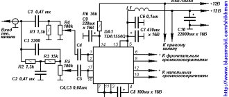
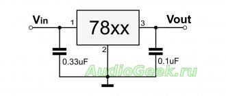
Thanks to a small number of wiring elements, the TDA2822M integrated circuit is one of the simple amplifiers that can be assembled in a short time, connected to an MP3 player, laptop, radio - and immediately evaluate the result of your work.
Here’s how attractive the description of the TDA2822M (ST, DIP8) chip looks at the Datagorsk fair: “TDA2822M is a stereo, two-channel low-voltage amplifier for portable equipment, etc. It can be bridged, used as a headphone or control amplifier, and much more. Operating supply voltage: 1.8 V to 12 V
, power up to 1 W per channel, distortion up to 0.2%. No radiator required. Despite its super-miniature size, it produces honest bass. The ideal chip for beginners' inhumane experiences."
With my article, I tried to help fellow radio amateurs make experiments with this interesting chip more conscious and humane.
↑ Let's look at the chip body
There are two microcircuits: one TDA2822, the other with the index “M” - TDA2822M. The integrated circuit TDA2822
(Philips) is designed to create simple audio power amplifiers.
The permissible range of supply voltages is 3…15 V; at Upit=6 V, Rн=4 Ohm, the output power is up to 0.65 W per channel, in the frequency band 30 Hz...18 kHz. The chip package is Powerdip 16. The TDA2822M chip
is made in a different Minidip 8 package and has a different pinout with a slightly lower maximum power dissipation (1 W versus 1.25 W for the TDA2822).
DIY transistor audio amplifier circuit
The range of sound frequencies that are perceived by the human ear is in the range of 20 Hz-20 kHz, but a device made on a single semiconductor device, due to the simplicity of the circuit and the minimum number of parts, provides a narrower frequency band. In simple devices, a frequency range of 100 Hz-6,000 Hz is sufficient for listening to music. This is enough to play music on a miniature speaker or earphone. The quality will be average, but quite acceptable for a mobile device.
The circuit of a simple audio amplifier using transistors can be assembled using silicon or germanium products of direct or reverse conduction (pnp, npn). Silicon semiconductors are less critical to supply voltage and have less dependence of characteristics on junction temperature.
↑ Functional diagram of TDA2822M
given in the documentation [1].
As can be seen from Fig. 1, each amplifier channel is close in structure to a typical Lin circuit. The amplifiers have common functional units: circuits for setting the reference current I REF for stable current generators (GCT) in the emitter circuits of differential stages, a circuit for setting the bias R3, D6 on the bases of keys Q12, Q13 and circuits for maintaining quiescent currents I0 CONTROL of the amplifier output stages.
This solution helps improve the stability of the amplifier in bridge mode. Each amplifier channel consists of a differential stage Q9…Q11 (Q14…Q16), a voltage amplifier Q7 (Q18) and an output stage Q1…Q6 (Q18…Q24).
Rice. 1. Functional diagram of TDA2822M from Datasheet
The differential cascade has a dynamic load in the form of a current mirror on elements Q8, D5 (Q17, D6).
Fragment excluded. The full version is available to patrons and full members of the community.
Please note that there are no other built-in protection circuits for the output stage, which is done for reasons of better use of the power supply, unfortunately at the expense of reliability.
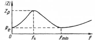
Pins 5 and 8 of the microcircuit are connected to the common wire via alternating current. In this case, the gain of the amplifier with negative feedback will be:
Ku=20lg(1+R1/R2)= 20lg(1+R5/R4)=39 dB.
The block diagram of the IS is shown in Fig. 2.
Rice. 2. Block diagram of TDA2822M
It was experimentally determined that the sum of the resistances of resistors R1+R2 and R5+R4 is equal to 51.575 kOhm. Knowing the gain, it is easy to calculate that R1=R5=51 kOhm, and R2=R4=0.575 kOhm.
To reduce the gain of an OOS microcircuit, an additional resistor is usually connected in series with R2 (R4). In this case, such a circuitry technique is “interfered” with open transistor switches on transistors Q12 (Q13).
But even if we assume that the keys do not affect the feedback gain, the maneuver to reduce the gain is insignificant - no more than 3 dB; otherwise, the stability of the amplifier covered by OOS is not guaranteed.
Therefore, you can experiment with changing the transmission coefficient of the amplifier, taking into account that the resistance of the additional resistor lies in the range of 100...240 Ohms.
Audio amplifier circuit with 1 transistor
The simplest audio amplifier circuit using a single transistor includes the following elements:
- Transistor KT 315 B
- Resistor R1 – 16 kom
- Resistor R2 – 1.6 kom
- Resistor R3 – 150 ohm
- Resistor R4 – 15 ohm
- Capacitor C1 – 10.0 µF
- Capacitor C2 – 500.0 µF
This is a device with a fixed base bias voltage, which is set by the divider R1-R2. The collector circuit includes resistor R3, which is the load of the cascade. Between pin X2 and the plus of the power source, you can connect a miniature speaker or earphone, which should have a high resistance. A low-impedance load cannot be connected to the cascade output. A correctly assembled circuit starts working immediately and does not need to be configured.
↑ Stereophonic and monophonic amplifiers on the TDA2822M chip
A wide range of supply voltages of 1.8…15 V allows the microcircuit to be “adapted” for a wide range of portable battery-powered devices.
It is easy to make both a stereo amplifier and a mono amplifier with a bridged microcircuit.
In this case, in the stereo version, the output power with a supply voltage of 6 V and the use of two speakers with a resistance of 4 Ohms will be 2x0.65 W, in the bridge version with a supply voltage of 9 V and a load resistance of 16 Ohms, it allows you to get 2 W of output power. In all cases, the harmonic coefficient will not exceed 0.2%.
↑ Experiments with a stereo amplifier
were carried out in accordance with the schemes shown in Fig.
3 and 8. The stereo amplifier shown in Fig. 3, can be used with both small speaker systems and headphones. Briefly about the purpose of the elements.
Resistors R1 and R2 determine the input impedance of the amplifier. Capacitors C1, C2 in the OOS circuit are connected in series with resistors R5, R6, which make it possible to reduce the gain in each of the amplifier channels within small limits. As mentioned above, the resistance of resistors R5, R6 can be in the range of 100...240 Ohms.
Since there is a constant voltage at the outputs of the UMZCH, approximately equal to half the voltage of the power source, the connection to the load is made through isolation capacitors C3, C4.
At the output of each channel, Zobel circuits R3, C6 and R4, C7 are included, ensuring stable operation of the amplifier. By the way, without these circuits the amplifier is inoperable.
Two capacitors are installed along the power supply circuit of the amplifier: ceramic C8 and oxide C5.
Fragment excluded. The full version is available to patrons and full members of the community.
Rice. 3. Schematic diagram of an experimental stereo amplifier
The amplifier has the following characteristics:
Supply voltage Up=1.8…12 V Output voltage Uout=2…4 V Current consumption in quiescent mode Io=6…12 mA Output power Pout=0.45…1.7 W Gain Ku=36…41 (39 ) dB Input impedance Rin=9.0 kOhm Crosstalk attenuation between channels 50 dB.
From a practical point of view, for reliable operation of the amplifier, it is advisable to set the supply voltage to no more than 9 V; in this case, for a load Rн=8 Ohm the output power will be 2x1.0 W, for Rн=16 Ohm - 2x0.6 W and for Rн=32 Ohm - 2x0.3 W. With load resistance Rн=4 Ohm, the optimal supply voltage will be up to 6 V (Pout=2x0.65 W).
The gain of the microcircuit of 39 dB, even taking into account a small downward adjustment by resistors R5, R6, turns out to be excessive for modern signal sources with a voltage of 250...750 mV. For example, for Up=9 V, Rн=8 Ohm, the sensitivity from the input is about 30 mV.
In Fig. 4, a shows the amplifier connection circuit, which allows you to connect a personal computer, MP3 player or radio receiver with a signal level of about 350 mV. For devices with an output signal of 250 mV, the resistance of resistors R1, R2 must be reduced to 33 kOhm; at an output signal level of 0.5 V, resistors R1=R2=68 kOhm, 0.75 V – 110 kOhm should be installed.
Double resistor R3 sets the required volume level. Capacitors C1, C2 are transitional.
Fragment excluded. The full version is available to patrons and full members of the community.
Rice. 4. UMZCH connection diagram: a) - to speaker systems, b) - to headphones (headphones)
In Fig. 4, b shows the connection to the amplifier of the headphone jack. Resistors R4, R5 eliminate clicks when connecting stereo phones, resistors R6, R7 limit the volume level.
During the experiments, I tried to power the UMZCH both from a stabilized power supply (on an LM317 integrated circuit and a BD912 transistor), Fig. 5, and from a battery with a capacity of 7.2 A•h for a voltage of 12 V with a power supply for fixed voltages, Fig. 6.
The supply voltage is supplied by as short a pair of wires as possible, twisted together. A correctly assembled device does not require adjustment.
Fragment excluded. The full version is available to patrons and full members of the community.
Rice. 5. Schematic diagram of a stabilized power supply
Fragment excluded. The full version is available to patrons and full members of the community.
Rice. 6. Rechargeable battery - laboratory power source
A subjective assessment of the noise level showed that when the volume control is set to the maximum level, the noise is barely noticeable. Subjective assessment of sound reproduction quality was made without comparison with the standard. The result is a good sound, listening to soundtracks does not cause irritation.
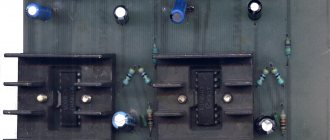
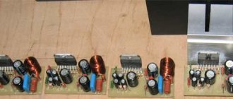
I checked the chip forums on the Internet, where I came across many messages about searching for unknown sources of noise, self-excitation and other troubles. As a result, he developed a printed circuit board, the distinctive feature of which is the “star” grounding of the elements. A photo view of the printed circuit board from the Sprint-Layout program is shown in Fig. 7.
Fragment excluded. The full version is available to patrons and full members of the community.
Rice. 7. Placement of parts on the experimental printed circuit board
During experiments on this signet, it was not possible to encounter any of the artifacts described on the forums.
Details of the stereo UMZCH on the TDA2822M chip
The printed circuit board is designed for installation of the most common parts: MLT, S2-33, S1-4 or imported resistors with a power of 0.125 or 0.25 W, film capacitors K73-17, K73-24 or imported MKT, imported oxide capacitors.
I used inexpensive but reliable electrolytic capacitors with low impedance, long service life (5000 hours) and the ability to operate at temperatures up to +105°C from Hitano ESX, EHR and EXR series. It should be remembered that the larger the outer diameter of the capacitor in the series, the longer its service life.
The DA1 chip is installed in an eight-pin socket. The TDA2822M chip can be replaced with KA2209B (Samsung) or K174UN34 (Angstrem OJSC, Zelenograd) [2, 3]. CHIP capacitor C8 (SMD) is located on the side of the printed tracks.
Details
DA1 - TDA2822M ST Housing: DIP8-300 - 1 pc., SCS-8 Narrow dip socket - 1 pc., R1, R2 - Res.-0.25-10k (Brown, black, orange, gold) - 2 pcs. , R3, R4 - Res.-0.25-4.7 Ohm (Yellow, purple, golden, golden) - 2 pcs., R5, R6 - Res.-0.25-160 Ohm (Brown, blue, brown, golden) - 2 pcs., C1, C2 - Cond.100/16V 0611 +105°C - 2 pcs., C3 - C5 - Cond.1000/16V 1021+105°C - 3 pcs., C6, C7 - Cond. .0.1/63V K73-17 - 2 pcs., C8 - Cond.0805 0.1µF X7R smd - 1 pc.
Many radio amateurs, not without reason, believe that it is best to include microcircuits in accordance with the Datasheet and use printed circuit boards offered by the developers. Below are diagrams and printed circuit boards made on the basis of the documentation with the only modification - to increase the stability of the amplifier, a film capacitor is connected in parallel with the oxide capacitor along the power supply circuit (Fig. 8, 9).
Fragment excluded. The full version is available to patrons and full members of the community.
Rice. 8. Typical circuit diagram for connecting a microcircuit in stereo mode
Fragment excluded. The full version is available to patrons and full members of the community.
Rice. 9. Placement of elements of a typical stereo UMZCH
Details of a typical stereo UMZCH
When installing elements on a printed circuit board, I advise you to use simple technological techniques described in the Datagorsk article [4].
Details
DA1 - TDA2822M ST Housing: DIP8-300 - 1 pc., SCS-8 Narrow dip socket - 1 pc., R1, R2 - Res.-0.25-10k (Brown, black, orange, gold) - 2 pcs. , R3, R4 - Res.-0.25-4.7 Ohm (Yellow, purple, golden, golden) - 2 pcs., C1, C2 - Cond. 100/16V 0611 +105°C - 2 pcs., C3 — Cond. 10/16V 0511 +105°C (Capacitance can be increased to 470 uF) — 1 pc., C4, C5 — Cond. 470/16V 1013+105°C — 2 pcs., C6 – C8 — Cond. 0.1/63V K73-17 - 3 pcs.
Electrical circuit diagram
In the distortion characteristics of these microcircuits, it is difficult to even count the number of zeros after the decimal point. Almost shocking. Using these microcircuits, one gets the impression that one cannot make anything better than a modern op-amp. So it turns out that the ULF must have an input part on a modern op-amp chip. Well, then, don’t have any voltage amplification stages - just amplify the current with simple repeaters, that is, do not spoil the signal from the microcircuit in any way. In this sense, the microcircuit has a gain sufficient for audio tasks, the maximum amplification frequency is simply phenomenal, and the output is relatively powerful. The final result is the following complete amplifier circuit - Fig. 1, practically implemented.
Rice. 1 Amplifier circuit.
The tone control is described in the article “Tone control with pseudo-bypass”, the volume control in the article “TCRG with adaptation to the tone control”.
In general, the scheme is relatively simple. This is achieved by the fact that the main nodes - RT, TCRG and ULF are inextricably linked - like a single complex - they have common elements. Accordingly, there are no pass-through capacitors, connecting elements, unnecessary signal amplification, etc. In the diagram, the main nodes are conventionally separated by dotted vertical lines. The ULF consists of two parts - a voltage amplifier (VA) on A4.1 and a current amplifier (CA) on A4.2 with unity gain. This division of the ULF into two parts has some advantage - it reduces the influence of general negative feedback (OOF, so disliked by many audiophiles), and reduces the likelihood of self-excitation of the ULF.
Supplying a signal to a non-inverting input (A4.2) also reduces the likelihood of self-excitation (from practice). Well, as they sometimes write, it improves sound quality - my opinion is the same. That is, returning the full output signal to the UT feedback reduces distortion. More precisely, it does not add distortion, as if the feedback signal was divided by resistors (for amplification). But such a circuit design required the use of an op-amp with an increased supply voltage, input and output voltage - LME49860. Expensive chip, but it works great.
The voltage amplifier on A4.1 has an adjustable gain using trimming resistor R19 for the desired amplifier power. Accordingly, the greater the power of the amplifier, the greater the resistance of this resistor will be. The current amplifier on A4.2 has unity gain. The rated power of the amplifier is about 20 W at 4 Ω. But, if you install more powerful output transistors and heatsinks, you can probably increase the power to 70 W at 4 Ω (but I haven’t tested it). The scheme is relatively simple - which is what is required.
Typically, thermal stabilization is performed on diodes or a transistor mounted on a radiator. But it does not always work correctly, especially on small radiators. Transistors may overheat or the quiescent current may drop to zero. And Darlington transistors almost always overheat at high volumes. Therefore, the thermal stabilization system of the terminal transistors is made in two stages - Fig. 1, highlighted in purple.
The first stage of thermal stabilization is, as usual, in temperature due to the heating of elements D1, D2, T1, T2 (a lot has been written about this on the Internet). And the second stage is unusual - additionally for through + output current by supplying a voltage proportional to the current from R29, R30, slightly opening transistors T1, T2 and, thereby, reducing the bias voltage to the bases of T3, T4. This double thermal stabilization allows you to more accurately maintain the quiescent current and through current, and prevent the through current from exceeding specified values or dropping to zero. But I had to install not just a transistor or diode on the radiator (as usual), but a small printed circuit board with elements soldered without drilling holes - Fig. 2.
Fig. 2 Photo of double thermal stabilization scarves for output transistors (in the center).
Elements of double thermal stabilization in Fig. 1 are highlighted in purple and separated by wavy lines - like real wiring going to this scarf. There is more labor involved here. But for me, for example, such thermal stabilization is the only way to ensure the operation of Darlington transistors (in other circuits), which overheat terribly. Well, and, of course, this circuit is also irreplaceable on small radiators. This circuit also has a second advantage - it is the ability to install a larger through current (including quiescent current). And a larger and more stable through current allows the output transistors to operate without cutoff at any volume and transient volume. That is, the work of ULF class AB will approach the work in class Economy A (Super A).
The sound quality will improve (there are articles about this on the Internet). Here the quiescent current is about 100 mA and, regardless of the volume, it changes slightly, never leaving the output transistors without through current and preventing them from overheating. It is better to calculate the quiescent current using Ohm’s law, measuring the voltage at points “I” and “K”. The quiescent current is regulated by resistors R27 and R28, the values of which must be the same. This double thermal stabilization circuit can be used in most amplifiers. Of course, the circuit itself of these amplifiers will have to be somewhat modified.
Capacitor C16 (Fig. 1) can be installed “just in case,” or it can be left out. It has almost no effect on the DC output voltage of the UT.
The next difference of the proposed amplifier is the additional inductance L6 (highlighted in brown), in contrast to the usually used only L5. Here, inductance L6, like L5 (as usual), performs the function of protection against self-excitation. But L6 and L5 also perform a second, very important function - they are “decoupling” the cable from the electrical potential to the speakers. After all, the cable to the speakers is a powerful antenna with its own radio potential on the air. And, if the amplifier is connected, for example, to a tuner, which has its potential from the antenna cable and is not at all weak, then a potential difference at radio frequencies arises between these antenna cables. This potential difference will settle directly through the housings (ground) of the devices on the sockets of the interconnect cable. It is not known exactly how the circuits will react to this radio signal, but the sound will definitely be spoiled.
Of course, at first it seems that the interconnect cable should have zero braid resistance in order to reduce the potential difference. But it is not so. Even if the interconnect cable has an ideal zero braid resistance, the potential difference can settle on the internal zero tracks of the printed circuit boards - that’s no joy. Perhaps for this reason they often write that an inexpensive interconnect cable sounds better than an expensive one. The whole point is what and how the circuit will react. But, after all, there is also its own electrical potential from the 220 V network or other devices connected to the amplifier - there are also their own potentials.
Therefore, in this ULF output and zero to the speakers are filtered from the radio frequency signal by inductors L5 and L6 - “decoupled” from the radio potential of the cables to the speakers. The interconnect cable could be simpler. Of course, you also need to have a surge filter to “decouple” the amplifier from the network potential. It would also be nice if all connected units had good filtering from the network potential. The inductors L5 and L6 themselves are wound without a core on a mandrel with a diameter of 10 mm and contain 10 turns each. Winding wire, diameter 0.85 mm. Winding is required in only one layer - Fig. 3.
Fig.3 Winding inductors L5 and L6 on sections of tube on the shanks of the amplifier output jacks.
Resistors R33, R34, constantly connected to the output (unlike the commonly used switches for headphones), although to a small extent, still perform the function of a Zobel circuit (like circuit R31, C28, there are articles on the Internet). It is even better to reduce the value of resistors R33, R34. Resistors R32, R35 were installed based on literature recommendations. Their purpose is not entirely clear to me - they do not change anything “by ear”.
The amplifier turned out to be completely not prone to self-excitation. I touched and soldered the elements directly under voltage - nothing bad happened. No matter how hard I tried to cause self-excitation with various speakers, cables, touching the input and elements, maximum volume, etc. – could not cause self-excitement. It simply doesn't exist.
The amplifier itself is mounted in a BBK-970 home theater housing - a friend gave me a faulty one - Fig. 4.
Fig. 4 Initial home theater unit VVK-970.
But in vain I shortened the case with a grinder - there is not enough space left for radiators, and accordingly the power of the proposed amplifier is forcedly low - Fig. 5.
Fig. 5 Shortened body of VVK-970.
The amplifier board was designed taking into account the recommendations of the article “Routing the ground with a Silver Fan” (available on the Internet). Here, the input sockets, neutral wires to the speakers, neutral terminals of all power capacitors, output transistors next to their power capacitors (each transistor has its own capacitor), neutral (ground) terminals to the case, to the low-voltage grounds of the switching power supply, to zero of the power supply itself, to the braids of shielded wires. Well, in general, to any point where ground is required, the wires are taken from this one point (but closer to their channel) - Fig. 6.
Fig. 6 Ground distribution from one point with a symmetrical arrangement of channels.
True, the point turns out to be very large in area, and this area needs to be paved (strengthened). For example, do not cut long leads of high-current capacitors and resistors, but bend them, pointing them towards each other and solder them - Fig. 7.
Rice. 7 Bending the leads (no soldering yet).
All braids of shielded signal wires must be grounded only at the zero point, even if these wires go past the zero point - Fig. 8.
Rice. 8 Braid soldering at the zero point.
It is necessary to remove part of the insulation on this wire, closer to the zero point, and solder it to the braid with a tap to the zero point. The braid itself always has resistance, which may have a detrimental effect on the sound. Therefore, the braid must be duplicated with wire (naturally to zero). All neutral wires are silver-plated - Fig. 9.
Rice. 9 Duplicating the cable braid with a separate wire (at the input jacks). The third wire goes to the “housing” screw.
From the zero point, it is necessary to cover all free areas of the board with a screen - do not etch copper from the board. This measure will reduce the various interferences of elements against each other, and will duplicate the zero somewhere.
In general, this layout resembles “dual mono”, because the channels are clearly on the right and left of the board. But there is an advantage of this wiring in that the lands of both channels are at one point, united. Accordingly, there will not be, although small, but still a potential difference between the zeros as with “double mono”.
Sometimes the question comes up: Is it justified to use a silver-plated wire for zero wiring? For me personally, the answer is clear. Yes. Justified. If you know for sure that copper wire is made of truly pure copper, then you can use it. For example, believing the information, it is made from highly purified oxygen-free copper. But it often happens that it is difficult to even tin copper wires - copper is contaminated with oxides, salts and much more.
Of course, after some effort, the wire is tinned and even soldered well, but where is the guarantee that after a couple of years of operation, the copper under the solder layer will not turn into oxides again? Approximately the same oxides can form simply along the depth of the copper wire, along its length - as on the surface during difficult tinning. This is a disaster for sound. Especially with long wires. I also had cases when the factory tinning layer on Soviet LEDs fell off like a crust. And under this crust there was some kind of dirt, which had to be scraped off for a long time in order to tin the output again. There was also foil-coated getinax, the copper of which, after five years of normal storage, turned into something dark brown in color.
Well, probably the most compelling example is when on Soviet TVs that had a quality mark, it was necessary to resolder a quarter of the pins of radio components on the boards with new tinning. Externally, the soldering of the part output is normal, but there is no contact. If you take a magnifying glass, you can see a dark round halo around the solder lead of the part - this is the insulating dirt that has formed.
When using silver-plated wire, all these outrages cannot happen. And the copper in them is of better quality. The insulation of silver-plated wires is also better - it does not melt, does not crack, and does not harm the sound. Well, and, of course, silver has less resistance - which is also better - there will be no unnecessary signal losses, no extra interference with elements, no unnecessary influence of elements on each other. Well, the most expensive interconnects and speaker cables are silver-plated. You can continue to list the benefits of silver.
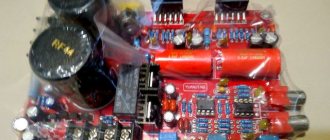
The amplifier board is experienced, so it is very ugly. I soldered a lot of things until the final version of the circuit, which does not correspond to the original idea. Therefore, I do not provide a sketch of the board. Almost all the radio components are used - I installed what I had. I came across solder, which always looks like a mess on the soldering iron. Apparently some fractions don’t really melt. Therefore, the soldering is simply terrible in appearance.
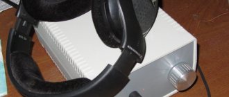
Listening to the amplifier showed that its sound is significantly, several times cleaner than the sound of my Grundig R1 - Fig. 10.
Fig. 10 Listening (comparison with Grundig).
According to Grundig's passport, the distortion is 0.008%. It’s a pity that I don’t have instruments to measure the quality indicators of amplifiers, so I can’t give any numbers. My main criterion for assessing the quality of an amplifier is the spatial perception of sound. Grundig up and down does little to separate sounds from the speakers. The sound is like a stripe from left to right between the speakers. The proposed amplifier expands the sound up and down. Sometimes, not only with closed, but also with open eyes, it is difficult to imagine where the sound is coming from. At the same time, the speakers are visible, but it is impossible to say that the sound is coming from them. Sounds are heard throughout the entire front hemisphere. Almost like wearing headphones.
For example, I had never noticed before that in Smokov’s song Stumblin’in, Chris Norman’s voice is geometrically higher than Suzi Quatro’s – apparently she is shorter. Both singers are clearly localized on stage. They stand side by side, like in the video clip of this song. You can hear who is on which side. On Grundig the voices are not localized at all and represent a large spot. It is very funny and surprising to hear the applause at the beginning of the concert composition Mistreated (Rainbow, On Stage -77). On the proposed amplifier, the applause claps go from the level of the speakers almost to the ceiling of the room. About the same as if there is a large chessboard on the wall and each clap has its own square. The distance between the speakers is 4 meters. It's simply amazing to listen to. Apparently the recording equipment was installed on the rear balcony facing downwards. Accordingly, the claps go up during playback.
On Grundig, the claps are vague and rise above the speakers by a maximum of 50 centimeters - the entire mesmerizing effect of the hall is lost. Another interesting aspect of the proposed amplifier is the complete absence of background and hiss in the speakers. When the signal source is turned off from the network (even if the amplifier input is short-circuited) and the volume control is at full volume, nothing can be heard near the speaker. You have to move your ear near the speakers for a long time to hear a subtle hiss. There is nothing at all from the woofer speaker. None of the amplifiers that I have ever heard have produced such silence. I couldn’t even believe that the amplifier was in working mode. In general, after the proposed amplifier I no longer want to listen to Grundig.
The tone control and loudness showed excellent performance, I would even say above expectations. When changing the timbre and turning the loudness on and off, the stage depth, space and simply sound quality do not change at all. As planned, the addition of low and high frequencies from loudness compensation is approximately the same as when simply adding low and high frequencies with timbre. But if you listen for a long time, then loudness compensation still gives a lower-frequency addition. This is probably theoretically correct, taking into account curves of equal loudness.
When the volume is reduced from maximum to minimum, the frequency balance “audibly” does not change. There is no desire to tweak the timbre. It often seems that loudness is even more important than the tone control. I don't want to listen without the loudspeaker turned on. The function of lowering the bass at maximum volume (with loudness compensation turned on) is well implemented, when the timbre of the bass is slightly reduced - the speakers are not overloaded. Grundig has all these indicators much worse. However, the Grundig BOX 5700 speakers showed their best side - Fig. 11.
Rice. 11 Grundig Columns.
When guys I knew who were music lovers listened to these speakers, they were surprised at the quality and the fact that they played better bass than modern speakers with a volume of 2 times larger and five times more expensive.
Listening to a friend's amplifier on a very high-quality signal source and very high-quality speakers (Fig. 12, 13) also showed its excellent performance.
Rice. 12 Listening to the amplifier on a quality source.
Rice. 13 Listening to the amplifier on high-quality speakers and a turntable.
For example, in the composition “The Happiest Days of our Lives”, Pink Floyd, The Wall, the sound of a helicopter rises above the speakers by no less than 70 centimeters. Not every piece of equipment lifts a helicopter so high. Overall the sound is very good.
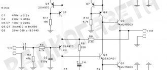
↑ Experiments with a bridge amplifier
were carried out according to the schemes shown in Fig.
10 and 12. In Fig. Figure 10 shows a diagram of an experimental bridge amplifier. Fragment excluded. The full version is available to patrons and full members of the community.
Rice. 10. Schematic diagram of an experimental bridge amplifier
Unlike the stereo amplifier circuit (Fig. 3), which assumes that coupling capacitors are present at the output of the previous device, a coupling capacitor is included at the input of the bridge amplifier, which determines the lower frequency reproduced by the amplifier.
Depending on the specific application, the capacitance of capacitor C1 can be from 0.1 μF (fn = 180 Hz) to 0.68 μF (fn = 25 Hz) or more. With capacitance C1 indicated on the circuit diagram, the lower frequency of the reproduced frequencies is 80 Hz.
Internal resistors connected to the inverting inputs of the amplifier through an isolation capacitor C2 are connected to each other, which provides output signals of equal magnitude but opposite in phase.
Capacitor C3 corrects the frequency response of the amplifier at high frequencies.
Since the DC output potentials of the amplifier are equal, it became possible to directly connect the load, without isolating capacitors.
The purpose of the remaining elements was described earlier.
For the stereo version, you will need two bridge amplifiers on the TDA2822M chip. The connection diagram is easy to obtain using Fig. 4.
Reliable operation of the amplifier in bridge mode is ensured by selecting the appropriate supply voltage depending on the load resistance (see table).
All parts of the bridge amplifier are placed on a printed circuit board measuring 32 x 38 mm made of one-sided foil fiberglass 2 mm thick. A drawing of a possible board option is shown in Fig. eleven.
Rice. 11. Placement of elements on the bridge amplifier board
Bridge Amplifier Parts
DA1 - TDA2822M ST Housing: DIP8-300 - 1 pc., SCS-8 Narrow dip socket - 1 pc., R1 - Res.-0.25-10k (Brown, black, orange, gold) - 1 pc., R2 , R3 - Res.-0.25-4.7 Ohm (Yellow, purple, golden, golden) - 2 pcs., C1 - Cond.0.22/63V K73-17 - 1 pc., C2 - Cond.10 /16V 0511 +105°C - 1 pc., C3 - Cond.0.01/630V K73-17 - 1 pc., C4 - C6 - Cond.0.1/63V K73-17 - 3 pcs., C7 - Cond. 1000/16V 1021+105°C - 1 pc.
The schematic diagram of a typical bridge UMZCH and the placement of elements on the printed circuit board are shown respectively in Fig. 12 and 13.
Fragment excluded. The full version is available to patrons and full members of the community.
Rice. 12. Typical circuit for connecting a microcircuit in bridge mode
Rice. 13. Placement of elements of a typical bridge UMZCH
Details of a typical bridge UMZCH
DA1 - TDA2822M ST Housing: DIP8-300 - 1 pc., SCS-8 Narrow dip socket - 1 pc., R1 - Res.-0.25-10k (Brown, black, orange, gold) - 1 pc., R2 , R3 - Res. -0.25-4.7 Ohm (Yellow, purple, golden, golden) - 2 pcs., C1, C3 - Cond. 10/16V 0511 +105°C (Capacity C3 can be increased to 470 µF) - 2 pcs., C2 - Cond. 0.01/630V K73-17 - 1 pc., C4 - C6 - Cond. 0.1/63V K73-17 - 3 pcs.
↑ List of sources mentioned
1. TDA2822M Dual low-voltage power amplifier 2. KA2209B 3. Nefedov A. Microcircuit KR174UN34 // Repair & Service, 2002, No. 10, p. 63. 4. Datagor article Do it yourself car amplifier using TDA8560Q, TDA1557Q, TDA8563Q. Detailed instructions for beginners