Hello! We continue the topic raised in my article “Input buffer and volume control for UMZCH. Part 1". On the Datagor forum, Vladimir ( vol2008
) raised the topic of a retro-structure amplifier [1, 2] and proposed his own version of a buffer stage for the final amplifier [3].
I also propose a variant of the buffer stage with a pseudo-push-pull follower.
↑ Possible options for implementing buffer cascades
are shown in Fig. 1a-d.
Rice. 1. Options for a buffer stage for a power amplifier: a) emitter follower, b) emitter follower with dynamic load, c) pseudo-push-pull emitter follower on transistors of the same structure, d) pseudo-push-pull emitter follower on complementary transistors
An emitter follower with a resistor in the emitter circuit (Fig. 1a) has the disadvantage that when the amplitude of the input signal increases, the limitation of one half-wave of the signal may occur earlier than the other [4].
During the positive half-wave of the input signal, the emitter current VT1 is divided between the resistances in the emitter Re and in the load Rн. During the negative half-wave, the current through Rн flows in the opposite direction.
To avoid limitation, the emitter current of transistor VT1 must always be greater than zero.
It is easy to show that the maximum peak amplitude of the output signal is related to the voltage at the emitter Uе and the load resistance Rн and emitter Re as follows: Uoutmax=UеRн/(Re+Rн).
For the circuit shown in Fig. 1a we get: Uoutmax = 7.5 0.62/(0.62+1.1) = 2.7 V.
The use of an active load in the emitter circuit allows you to eliminate the disadvantage of an emitter follower with a resistive load and further reduce distortion (Fig. 1 b). Part of the disadvantage of a simple emitter follower remains here: with a positive half-wave of the input signal, current is supplied not only to the load, but also to the current source.
Pseudo-push-pull repeaters can significantly reduce all types of distortion, as well as the output impedance. Here, a controlled current generator is used as an emitter load, forming a counter dynamic load for the second arm, Fig. 1st century
Shown in Fig. 1c diagram – transfer of a patent for a tube repeater from the forties of the last century to transistor circuitry [5].
Since transistor circuitry, unlike lamps, uses transistors of two types of conductivity, this circuit can be modified, resulting in a complementary pseudo-push-pull follower, Fig. 1 g. This scheme was successfully used by Vladimir ( vol2008
).
The low output impedance of the circuits shown in Fig. 1c and fig. 1 g, as well as less distortion compared to the circuits shown in Fig. 1a and fig. 1 b, have a positive effect on sound reproduction.
PRINCIPLE DIAGRAM.
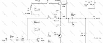
The schematic diagram of the buffer is shown in the figure:
Click to enlarge
Briefly, the essence of the method is this. Transistors T3 and T4 are a current mirror. Their output currents power the input and output transistors. Thus, a change in current through one transistor (Q1) causes a similar change in current through the other (T2). Due to the fact that the transistors are complementary, mutual compensation occurs for the nonlinearity of their characteristics.
↑ Buffer amplifier with level control based on a pseudo-push-pull repeater
In Fig.
Figure 2 shows a two-channel buffer amplifier with a level controller based on a pseudo-push-pull repeater, Fig. 1st century Here, instead of an emitter follower, a Szyklai circuit is used on transistors VT1, VT3 (VT5, VT4 in another channel). Fragment excluded. The full version is available to patrons and full members of the community.
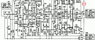
Rice. 2. Schematic diagram of a buffer stage with a pseudo-push-pull repeater
The collector current of transistor VT1 (VT5) is set by resistor R5 (R11) and is I0=Ube/R5=0.2 mA, where Ube=0.66 V is the base-emitter voltage of transistor VT3 (VT4).
The current sources are made on transistors VT2 (VT6), the base circuits of the transistors are powered by a common parametric voltage stabilizer HL1, R8, C3 through resistors R7 and R9, respectively. The current source current is 10 mA.
The antiphase signal from resistor R4 (R10) through the separating capacitor C2 (C4) is supplied to the base of the current source transistor VT2 (VT6), which ensures the active operating mode of the repeater on both half-waves of the input signal.
↑ Characteristics
Supply voltage: 15 V;
Current consumption: 25 mA; Lower frequency level – 0.5 dB: 1 Hz; Output impedance: 0.5 ohm; Harmonic coefficient in the entire range of operating frequencies (20...20000 Hz) at Uin=1 V, Rн=620 Ohm: no more than 0.001%. Compare the technical characteristics of the pseudo push-pull repeater with the design from [2]. The pseudo-push-pull buffer has a six-fold lower output impedance, and non-linear distortion has decreased seventeen times!
Input resistance of the buffer stage Rin = 47 kOhm. If necessary, oxide capacitors C1 (C5) at the repeater inputs can be replaced with film capacitors, for example, with a capacity of 1 μF or 2.2 μF; at the same time, the lower frequency level - 3 dB will remain acceptable (3.4 Hz and 1.5 Hz, respectively).
↑ Details of the pseudo-push-pull repeater
VT1, VT2, VT5, VT6 – Transistor BC546 – 4 pcs., VT3, VT4 – Transistor BC556 – 2 pcs., HL1 – LED red d=3 mm BL-B51V1 – 1 pc., R1, R14 – Res.-0, 25-82 kOhm (Grey, red, orange, golden) – 2 pcs., R2, R15 – Res.-0.25-110 kOhm (Brown, brown, yellow, golden) – 2 pcs., R3, R4, R6, R10 , R12, R13 – Res.-0.25-100 Ohm (Brown, black, brown, golden) – 6 pcs., R5, R8, R11 – Res.-0.25-3.3 kOhm (Orange, orange, red, golden) – 3 pcs., R7, R9 – Res.-0.25-1.0 kOhm (Brown, black, red, gold) – 2 pcs., R16 – Res.-0.25-10 Ohm (Brown , black, black, gold) – 1 pc., C1, C5 – Cond. 10/25V 0511 +105°C– 2 pcs., C2, C3, C4 – Cond. 100/25V 0812 +105°С – 3 pcs., C6 – Cond. 1000/25V 1021 +105°C – 1 pc. Printed circuit board 54×54 mm – 1 pc.
↑ Repeater board
All parts of the pseudo-push-pull repeater are placed on a printed circuit board made of single-sided foil fiberglass 2 mm thick (Fig. 3).
Fragment excluded. The full version is available to patrons and full members of the community.
↑ Assembly and adjustment
First, fixed resistors and a jumper are installed, then, observing the polarity and pinout, capacitors, transistors and an LED.
The last thing to install on the board is a variable resistor. The setup comes down to checking the DC modes shown in Fig. 2. Adjustment of modes, if necessary, can be carried out by selecting resistors R1 (R14).
CHARACTERISTICS OF THE SCHEME.
- Total harmonic distortion: typical value less than - 0.001%, measured on a prototype -
0.00025%! - Linear Distortion: Distortion doubles at frequencies above 55KHz and then doubles every octave thereafter.
- Noise Level: Below 138db at 1kHz
- Frequency band: more than 50 MHz (depending on the transistors used).
- Signal limit: +4.9V -6.3V
- Maximum output current: -10mA
- Input impedance: 10k - 100k (depending on input circuits, see below).
- Output impedance:<52R.
- Output zero offset: less than 5 mV.
↑ List of sources mentioned
1. Mosyagin V., Silicon versus germanium in amplifiers of the same retro structure and a new germanium whale at the end // Journal of practical electronics "Datagor", 2016. 2. Mosyagin V., Input buffer and volume control for UMZCH // Journal of practical electronics “Datagor”, 2016. 3. Classic UMZCH (PowerAmplifier) circuit based on “Datagor” transistors // Forum on Datagor.
4. Rysin A. How to avoid signal limitation in an emitter follower with capacitive load decoupling // Radio pilot, 2015, April, p. 54 – 57. 5. White E. Improvements in or relating to thermionic valve amplifier circuit arrangements, British patent no. 564.250 (1940). 6. Petrov A. Pseudo-pull output stages of class A. // Radiohobby, 2014, No. 4, p. 57 – 61. Thank you for your attention!
Content
- 1 Voltage buffer
- 2 Current buffer
- 3 Voltage buffer examples 3.1 Op-amp implementation
- 3.2 Single-transistor circuits 3.2.1 Impedance conversion using a bipolar voltage follower
- 3.2.2 Impedance conversion using MOSFET voltage follower
- 3.2.3 Circuit of single-transistor amplifiers
- 3.2.4 Logic buffer amplifiers
- 3.2.5 Loudspeaker Array Amplifiers
- 3.2.6 Managed security
- 4.1 Single-transistor circuits
Construction and details.
For ease of repetition, the Editor-in-Chief of RadioGazeta has developed a printed circuit board for the device (45mm X 45mm):
You can download the PCB drawing in Layout format here.
Inductance L1 is a ferrite bead. To ensure high thermal stability of the cascade, transistors T1-T3 and T2-T4 need to be glued in pairs with their rear walls. This is what it looked like on the layout:
Op amp feedback
As I already mentioned, operational amplifiers are almost always used with feedback (OS). But what is feedback and what is it for? Let's try to figure this out.
We encounter feedback all the time: when we want to pour tea into a mug or even go to the toilet for a small need.