What is an amplifier?
Low power signals are very common in electrical circuits. For example, this could be an audio signal from a dynamic microphone
weak radio signal that your Chinese radio picks up from the air
Or a reflected signal from an enemy missile, which is then caught, amplified and tracked by a radar installation. For example: TOP anti-aircraft missile system:
As you can see, in electronics absolutely everywhere there is a need to amplify weak signals. In order to amplify them, you need signal amplifiers. Amplifiers are widely used in radar, television, radio broadcasting, telemetry, computer technology, automatic control, automation systems, etc.
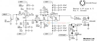
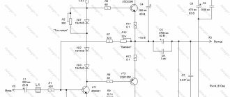
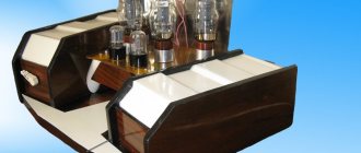
Some features of the experimental tract.
The path uses wires and components from Telefunken and Siemens receivers from the 30s-40s.
feed-through capacitors : copper foil, three-layer dielectric: “paper - thin packaging polyethylene - paper” because direct contact of the dielectric (including oil) and the conductor negatively affects the color of the component. In the case of a dry dielectric, this can be corrected by placing paper or cotton cloth between the conductor and the dielectric. The capacitor terminals are connected to the foil without soldering - the roll is simply twisted tightly and tightly tightened with cotton tape. Both the conclusions and the foil take into account the directions.
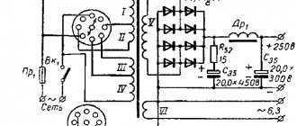
Rectifier - Full Wave [12] - When using a standard full wave circuit and a standard mains transformer, one of the transformer windings will be in the wrong direction. Parallel signal paths also have a detrimental effect on sound quality.
Resistors - The mounting wires are connected directly to the graphite coating, taking into account the directions of both the wires and the graphite coating.
Lamp sockets, audio and network connectors - (!) All connector blades are directional. The panels are assembled using petals with the required directions according to the diagram in Fig. 1. RSA connectors, both “female” and “male” on the interconnect cable, are used from various manufacturers, also with the necessary directions.
Signal source - to achieve the shortest possible path, the signal is taken directly from the output pins of the DAC.
Loudspeaker – “Noema” – 75GDSh33–16. It is rewound with Telefunken wire of a suitable diameter and, without breaks, is brought directly to the output contacts (in the area from the diffuser to the output contacts where “Litz” is usually used, the wire is twisted in the likeness of a telephone cord and glued with rubber glue).
Musical material - master discs produced using AML+ technology and others with successful remastering of recordings from the 40s-60s.
(!) Wherever possible, twists are used instead of soldering. (Soldering greatly impairs clarity - even with a total number of solders in the path of 20 pieces, getting rid of each of them makes a very serious contribution to improving the sound of the path. If there are more than 30-40 solders in the path, then its clarity suffers so much that it is difficult to distinguish by ear twisting from soldering is quite problematic). Feed-through capacitors and signal wires are removed from the steel chassis by at least 5 mm (otherwise the clarity and legibility of the color on the HF is lost). This indirectly confirms the negative impact of shielded wires on sound [13]. Only single-core wires were used (in stranded wires, very often the strands are laid in more than one direction, so the sound of stranded wires greatly depends on the place of contact and is always less clear than that of one individual core of the same cable).
Anton Stepichev.
Saint Petersburg,
June 28, 2005
The author expresses his gratitude to A. Likhnitsky for his assistance in writing the article.
_________________________________________________________________
[1] – A.M. Likhnitsky Reflections on the color of sound, AM No. 1 (48), 2003 pp. 160-163.
[2] -FEToole. Listening test – Turning Option into Fact. – JAES, V.30, No. 6, 1982, p.431-445.
[3] – Established by Oleg Khavin (previously stated on the forum www.aml.nm.ru)
[4] – Established by Anatoly Likhnitsky (previously stated on the forum www.aml.nm.ru)
[5] – Established by Evgeny Komissarov (previously stated on the forum www.aml.nm.ru)
[6] – Details about the levels of perception: A.M. Likhnitsky “Sound quality – a new approach to testing audio equipment.” "Peak" St. Petersburg 1998 pp. 13-20
[7] – A.M. Likhnitsky “How to talk about what we hear” AM No. 5 (10) 1996 p. 45.
[8] – A.M. Likhnitsky “On testing audio cables” AM No. 2 (3) 1995 p. 43.
[9] – A.M. Likhnitsky “On testing audio cables” AM No. 2 (3) 1995 p. 44.
[10] – In complex transistor circuits, HF composure is the only guideline. The sound begins to “come to life” only upon reaching a certain threshold, which is quite difficult to achieve using transistor technology with multi-way speaker systems. Once this threshold is reached, the correct direction can be determined even by telephone, which is confirmed by the experiments of Anatoly Likhnitsky
[11] – “Record Alive” Interview with A.M. Likhnitsky AM, No. 1/1994
[12] – The fact that the sound of a half-wave rectifier is preferable to a standard full-wave rectifier was first determined by Sergey Shabad.
[13] – Established by Oleg Khavin (previously stated on the forum www.aml.nm.ru)
What is a black box in electronics
In general, an amplifier can be viewed as a black box.
What is this black box? This is a box. He's black). And since it is black, absolutely no one knows what is in it. We can only guess. But it is also possible that we can take some action and wait for a response. After the response of this black box, we can guess what is inside it.
That is, in essence, a black box must have some “sensors” for perceiving information from the outside, some “input”, as well as some “output” for a response. That is, by applying any influence to the input, we wait for the response of the black box at the output.
Let there be a cat or cat in the black box, but so far no one knows that he/she is there. What will we do first? Let's shake the box or kick it, right? If someone meows there, it means it’s definitely either a cat or a male cat). That is, there was a response. How to determine further whether it is a cat or a male cat? We open the box, and a shaggy miracle crawls out of it. If it runs, it means it's a cat. If it runs, it means it’s a cat).
But there can also be absolutely any body or substance in the black box. For such situations, we must conduct as many experiments as possible, that is, produce as many input influences as possible to more accurately determine the contents of the black box.
Classes G and H
Another pair of designs designed for efficiency. From a technical point of view, neither Class G nor Class H amplifiers are officially recognized. Instead, they are variations on the Class A/B theme, using bus voltage switching and bus modulation respectively. In either case, in low demand conditions the system uses a lower bus voltage than an equivalent Class A/B amplifier, significantly reducing power consumption. When high power conditions occur, the system dynamically increases the bus voltage (that is, switches to the high voltage bus) to handle high amplitude transients.
There are also disadvantages. The main one is the high cost. Original network switching circuits used bipolar transistors to control the output flows, which adds complexity and cost. High-quality tube audio amplifiers of this type are common, although the price starts from 50 thousand rubles. The block is considered a professional technique for working on stage or recording in the studio. There are problems with transistors. Under prolonged load, some of them may fail.
Today, the cost is often reduced to some extent by using high current MOSFETs to select or change the guides. Using MOSFETs not only improves efficiency and reduces heat, but also requires fewer parts (usually one device per thread). In addition to the cost of bus switching, the modulation itself, it's also worth noting that some Class G amplifiers use more output devices than a typical Class A/B design.
One pair of devices will operate in typical A/B mode, powered by low voltage buses. Meanwhile, the other is kept in reserve to act as a voltage amplifier, activated only depending on the situation. Only classes G and H, associated with high-power amplifiers, can withstand high loads, where the increased efficiency pays off. Compact designs can also use Class G/H topologies as opposed to A/B, given that the ability to switch to low power mode means they can get by with a slightly smaller heatsink.
What is a quadripole
In electronics, a black box is a quadripole . What is a quadripole anyway? A four-terminal network is a black box containing an unknown electrical circuit inside. Here we see two input terminals, through which the input action is supplied, and two output terminals, from which we will now take the response of our “electric black box”.
Passive quadripole
For example, an RC circuit is a passive four-terminal network , since it has four terminals: two for input and two for output, and as we can see, it does not contain any power supply. This RC circuit is a passive low pass filter (LPF).
In passive two-terminal networks, the voltage or current at the output can be greater than at the input, but the power does not increase. How can the voltage or current at the output be greater than at the input? Here it is enough to recall the transformer, as well as series and parallel oscillatory circuits. For them, it would be more accurate to define a voltage converter, but not an amplifier, since the amplifier must include a power source from which it will take energy to amplify a weak input signal.
Also, in a passive four-port network, the output power will in no way be greater than the input power. If you achieve this, you will immediately receive an eternal source of energy and a Nobel Prize to boot. But remember that the law of conservation of energy, which was first formulated by Leibniz in the 17th century, has not been canceled.
Active quadripole
But we will now call this four-terminal network active , since it includes a power supply +Upit, which is required in order to amplify the signal.
That is, here we see two terminals for the input, to which the signal Uin is driven, and we also see two terminals for the output, where the voltage Uout is removed. Our four-port network is powered via + Upit, as a result of which, in this case, the output signal will be greater than the input signal.
By driving a sinusoid into the input of such a circuit, at the output we will get the same sinusoid , but its amplitude will be many times greater.
This is, of course, true for an ideal amplifier, i.e. absolutely linear and without restrictions on the amplitude of the input and output signals. In real amplifiers, it is required that the amplitude does not exceed the permissible value and that the amplifier is properly designed. In addition, any real amplifier introduces distortion and is characterized by nonlinear distortion coefficient (THD) and many other parameters, which we will consider in the next article.
In an active four-port network , one of which is a power amplifier, the output power will be greater than the input. Naturally, this does not violate the law of conservation of energy, since the power released to the load is the converted power of the power source. The small signal input simply controls this power. You can read more in the article about the principle of transistor amplification.
In electronics, we will consider an amplifier as an active four-port network , to the input of which a low-power signal Uin is supplied, and a load Rн is attached to the output.
Class A
Compared to other classes of audio power amplifiers that will be described below, Class A models are relatively simple devices. The defining operating principle is that all transducer output blocks must pass through a full 360-degree signal cycle.
Class A can also be divided into single-ended and push-pull amplifiers. Push/pull differs from the basic explanation above by using output devices in pairs. While both devices perform a full 360-degree cycle, one device will carry most of the load during the positive part of the cycle, while the other will carry more of the negative cycle.
The main advantage of this design is reduced distortion compared to single-ended designs since even order oscillations are eliminated. In addition, Class A push-pull designs are less sensitive to noise.
Due to the positive qualities associated with Class A performance, it is considered the gold standard for sound quality in many areas of the speaker industry. However, these designs have one important drawback - efficiency.
The requirement for audio amplifiers using Class A transistors is that all output devices operate continuously. This action leads to significant energy losses, which are ultimately converted into heat. This is further compounded by the fact that Class A designs require relatively high levels of quiescent current, which is the amount of current flowing through the output devices when the amplifier is producing zero output. Real world efficiency rates can be on the order of 15-35%, with single digits possible using highly dynamic feedstock.
Generalized amplifier circuit
It looks something like this:
As we can see in the diagram, some source of a weak signal with EMF EI and internal resistance RI is connected to the input of the amplifier stage through terminals 1 and 2. It is this weak signal from this source that we will amplify. Further, as expected, each amplifier has its own input resistance Rin. The current strength Iin in the circuit EI -> RI -> Rin, as difficult as it may be to guess, will depend on the input resistance of the amplifier stage Rin.
As you already know, the power supply plays a major role in the amplifier stage. A low-power, weak signal controls the energy consumption of the power supply. As a result, at the output we get an amplified copy of the weak input signal. The amplification occurred due to the fact that the power supply provided its power to amplify the input signal. Well, something like this).
In the output circuit of the amplifier we receive an amplified signal with EMF (What is EMF) Eout and output resistance Rout. Through terminal blocks 3 and 4 we connect the load Rн, which will already consume the energy of the amplified signal. The current strength in the circuit Eout -> Rout -> Rн will depend on the load resistance Rн.
Class A/B
A tube audio amplifier can be found at many concert venues. It has high performance and does not overheat. In addition, the models are much cheaper than many digital blocks. But there are also deviations. This module may not work with all audio formats. Therefore, it is better to use the equipment as part of a general signal processing complex.
Class A/B combines the best of each device type to create a unit without the disadvantages of either. Thanks to this combination of advantages, Class A/B amplifiers largely dominate the consumer market.
The solution is actually quite simple in concept. Where Class B uses a push-pull device with each half of the output stage conducting 180 degrees, Class A/B mechanisms increase this to ~181-200 degrees. This way there is a much lower chance of a "break" occurring in the loop, and therefore the crossover distortion is reduced to the point where it doesn't matter.
Tube audio power amplifiers can absorb this interference much faster. Thanks to this property, the sound coming out of the device is much cleaner. Models of similar characteristics are often used to transform the sound of acoustic and electric guitars.
Suffice it to say that Class A/B delivers on its promise, easily outperforming pure Class A designs with performance rates on the order of ~50-70% achieved in the real world. Actual levels, of course, depend on how much the amplifier is biased, as well as on the program material and other factors. It's also worth noting that some Class A/B designs go one step further in their quest to eliminate crossover distortion by operating in pure Class A mode up to a few watts of power. This gives some efficiency when running at low levels, but also ensures that the amp doesn't turn into a furnace when delivering large amounts of power.
Amplifier types
Amplifiers can be divided into three groups:
Voltage amplifier
A voltage amplifier (VA) amplifies the input voltage a specified number of times. This coefficient is called voltage gain and is calculated by the formula:
Where
KU is the voltage gain
Uout - amplifier output voltage, V
Uin - voltage at the amplifier input, V
The output amplified voltage should not change from the load current, and therefore from the load resistance. Ideally, the output resistance Rout should be zero, which is unattainable in practice. Therefore, they try to design NAs in such a way as to minimize the output resistance Rout.
In this mode, the amplifier operates if the conditions are met that Rin is much greater than Rout, i.e. Rin >>Ri and Rn are much greater than Rout (Rn >>Rout). The higher the rating Rн, the better for the voltage amplifier, since the load will not sag the output voltage Uout. Everything is simple here: the lower the load resistance, the greater the current will flow through the circuit Eout -> Rout -> Rn, the greater the voltage drop across the output resistance Rout, based on the EMF formula: Eout = IoutRout + IoutRn. You can read about this in more detail in the article Ohm's Law for a complete circuit.
Current amplifier
The current amplifier (CA) amplifies the input current by a specified number of times. This coefficient is called the current gain and is calculated by the formula:
where KI is the current gain
Iout - current strength in the load circuit, A
Iin - current strength in the input circuit Ei ->Ri ->Rin, A
The meaning of the operation of the current amplifier is this: at a certain current strength in the input circuit, at the output in the load circuit we obtain a current strength that is KI times greater, regardless of what value the load rating takes. Ohm's simple law I=U/R already works here.
If the current strength must be constant, and our resistance value can be floating, then to maintain a constant current strength in the load circuit, our amplifier automatically changes the voltage Uout at the load. As a result, the current remained constant and remained the same. Or in letters: Rн =var, Iout= const.
You will tell your electronics teacher the above explanation, and now the explanation is for complete dummies . So, in the input circuit Ei -> Ri -> Rin, let us have a current flow of 10 mA. Coefficient KI = 100, therefore, at the output in the load circuit Eout -> Rout -> Rн a current with a force of 1 A (10 mA x 100) will flow. But such a current by itself will not flow through this circuit. It needs to create conditions for it to occur. Let's say we have a load of 10 ohms. What then should be the voltage in this circuit to obtain a current in this circuit of 1 A? Remember Uncle Om: I=U/R. 1=Uout/10, we get U=10 V. This is the voltage the current amplifier will give us at the output.
But what if the load changes its value? The current should remain the same, do not forget, that is, 1 A, since this is a current amplifier. In this case, so that the current in the circuit remains 1 A, the amplifier will automatically change its voltage value at the output Uout to 1=Uout /5. Uout =5/1=5 V. That is, we will already have 5 Volts at the output.
But we also do not forget about one more parameter, which is located in the output circuit of the current amplifier. This is the output resistance Rout. Therefore, we need the following condition to be satisfied: Rin << Ri and Rn << Rout at which the specified current in the load is ensured at a low voltage value.
Amplifier
It used to be very cool and fashionable to assemble power amplifiers (PA) with your own hands, turn on Tender May and turn the volume up to full blast. Now everyone can assemble or buy UM, since the Internet and Aliexpress are always at hand.
How does UM differ from UN and UT?
If in the UT we increased only the current, in the UN we increased the voltage, then in the UM we increased the current and voltage by a multiple of times.
The power formula for direct and alternating current with a resistive load looks like this:
Where
P—power, W
I - current strength, A
U—voltage, V
Therefore, the power gain will be written as:
Where
KP - power gain
Pout - amplifier output power, W
Pin - power at the amplifier input, W
For a power amplifier, the conditions for matching the input circuit with the source of the input signal and the output circuit with the load for transmitting maximum power have the form: Rin ≈ Ri and Rn ≈ Rout.
Also, do not forget that loads can be either purely active (such as an incandescent light bulb, a resistor, various heaters) or have a reactive component (inductors, capacitors, motors, etc.).
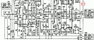
It is well known that the sound quality of any sound reproducing complex largely depends on the parameters of the audio frequency power amplifier (AMP). To date, many versions of transistor UMZCH have been published, sometimes distinguished by very high quality indicators, but the search for new circuit solutions that make it possible to bring the sound of sound-reproducing devices even closer to natural continues. This article discusses some ways to improve UMZCH on a modern element base.Despite the variety of transistor UMZCH circuits, the principles of their construction are practically the same. Like modern integrated op-amps, they are usually two-stage (Fig. 1). The main voltage gain is provided by the first two stages. The output stage is most often a powerful voltage follower, which is why this UMZCH configuration is called two-stage.
The criterion for the quality of UMZCH is the nature and magnitude of the distortions it introduces. Let's try to classify the currently known distortions of the AF signal.
First of all, let us pay attention to the imperfection of which characteristics is caused by one or another type of them. For this purpose, we divide distortions into static and dynamic (see Fig. 2). The former are caused by the nonlinearity of the static transfer characteristics of UMZCH cascades (for example, the nonlinearity of the input and output characteristics of the amplification elements used), the latter by the non-ideality of their transient characteristics, which is understood as the response of the amplifiers to a jump in input voltage. Static distortions, in turn, can be divided into harmonic, expressed in a change in the shape of the original signal of a certain frequency, and intermodulation, manifested in the enrichment of the spectrum of the output signal with combinational components.
Static intermodulation distortions can be amplitude and phase (determined, respectively, by the mutual amplitude and phase modulation [1-3] of the input signals). Dynamic distortion can also be divided into harmonic and intermodulation. In the first case, we are talking about distortions in the shape of the input sinusoidal signal when its amplitude and frequency exceed critical values determined by the maximum rate of rise of the output voltage. If, under these conditions, signals of other frequencies are also present at the input of the UMZCH, then conditions arise for the occurrence of strong intermodulation distortions.
As already mentioned, dynamic distortion depends, in particular, on such a parameter as the rate of rise of the output signal Vu, which is related to the maximum frequency fv of the amplified signal of maximum amplitude by the relation Vu = 2πfBUm, where Um is the maximum amplitude of the output voltage. If we take into account that the output sinusoidal power is P=Um2/2RH, where RH is the load resistance, then we can get Vu=2πfв√2PRн.
Let us estimate the rate of rise of the output voltage necessary for undistorted sound reproduction if, for example, all spectral components of the amplified signal are below 20 kHz, and the power of the amplifier at a load with a resistance of 4 Ohms is 100 W. In this case, according to the above formula, Vu=3.6 V/µs. A further increase in the slew rate has virtually no effect on dynamic distortion in the audio frequency band [4].
The above classification is convenient in that it allows us to most fully characterize the distortions introduced by the amplifier. It should be borne in mind that all types of distortions are interrelated. For example, a change in harmonic distortion will inevitably affect intermodulation distortion, etc.
The human ear is most sensitive to intermodulation distortion. Their visibility largely depends on the type of music program. Psychoacoustic studies have shown [5] that highly qualified experts began to notice changes in the character of the piano sound as soon as the root mean square value of intermodulation distortion reached 0.003% (!). For comparison, we point out that the threshold for noticeable distortion of the sound of a choir is 0.03%, for a violin - approximately 0.3%.
Let us now consider ways to improve individual UMZCH cascades in order to build a device with minimal distortion.
The input stage determines such important parameters of the UMZCH as the “zero” mixing voltage (the constant component of the amplifier’s output voltage) and its temperature stability. The maximum rate of rise of the output voltage and the signal-to-noise ratio largely depend on the circuit design of this stage. In the vast majority of modern UMZCHs, the input stage is differential. The requirements for it are determined by the type of environmental protection covering the entire UMZCH. Let's compare inverting (with parallel feedback) and non-inverting (with series feedback) amplifiers. The gain of a non-inverting amplifier (Fig. 3,a) is KU=1+R3/R2, and an inverting amplifier (Fig. 3,b) is KU=R3/R2. The advantage of a non-inverting amplifier is its high input resistance, which is limited by the resistance of resistor R1 (200 kOhm), while for an inverting amplifier it is almost equal to the resistance of resistor R2 (10 kOhm).
However, when analyzing the linearity of the input stages (Fig. 1), the advantages are on the side of the inverting amplifier, and here's why. With a sufficiently large gain of the UMZCH with an open circuit OOS, the voltages at the inverting and non-inverting inputs are almost the same. For example, if a 1 V input signal is received at the input of a non-inverting amplifier, then the same voltage will be at its inverting input. In other words, at the inputs of the amplifier there is an alternating common-mode voltage with an amplitude of 1.4 V. It is easy to see (see Fig. 1) that the voltage of the current source GI1 and the collector-emitter voltage of transistors VT1 and VT2 of the input differential stage will fluctuate with a swing of 2 .8 V. This parasitic modulation leads to a nonlinear change in the parameters of the transistors in time with the input signal, which creates the preconditions for the occurrence of additional distortions, and first of all, non-thermodulation ones. In an inverting amplifier, the common-mode component is practically zero and the above-described distortions do not occur.
To eliminate the influence of the common-mode component and reduce the distortion of a non-inverting amplifier, it is necessary to increase the output resistance of the current source and select a pair of transistors with the closest possible parameters to the differential stage [6]. In cases where the value of the common-mode component reaches several volts, instead of a conventional single-transistor current source, it is advisable to use a more advanced current source on two transistors VT5, VT6 (Fig. 4) (3, 7]. An integrated assembly is used as a differential pair VT3, VT4 K159NT1. transistors of which have close values of the static coefficient h21E and emitter-base voltages. To reduce the operating voltage of the transistors of the assembly (the permissible voltage between their collectors and emitters is 20 V), higher voltage transistors VT1. VT2, connected according to the circuit with OB, are introduced into the collector circuits Resistors R5, R9 also help reduce dynamic distortion [8].
The main way to improve the quality indicators of UMZCH remains the introduction of deep OOS, which is possible with a sufficiently large gain of the original (without OOS) amplifier. The gain of a typical input differential stage is 10 ... 26 dB. It can be increased by replacing the passive load in the collector circuits of transistors VT1, VT2 (Fig. 4) with an active one. Its functions can be performed by the so-called “current mirror” (Fig. 5, a) or “current mirror” with tracking feedback (Fig. 5, b). It is easy to see that in the latter case, the voltage between the base and collector of transistor VT2′ is equal to the voltage at the emitter junction of transistor VT3′. Due to this, the voltage drop in the emitter-collector section of transistor VT2′ does not exceed 1.3 ... 1.4 V. The voltage between the emitter and the collector of transistor VT1′ depends on the voltage amplification stage, but it, as a rule, does not exceed 3 V. All this allows the use of transistors with a low permissible collector-emitter voltage in the “current mirror”, in particular, the KTS3103A transistor assembly.
It should be noted that in order to realize the large gain that a differential stage with such a load can provide, the input impedance of the next stage must be quite high.
In the input stage according to the diagram in Fig. 4 you can use KT312V transistors. KT315V. KT315G and KT3102B and transistor matrices of the K198 series (K198NT1—K198NT4). Zener diode VD1 can be replaced with KS139A, VD3 with KS175A or KS168A (in the latter case, the resistance of resistor R7 must be reduced to 3.3 or 3 kOhm, respectively, and resistor R3 must be increased to 3.9 kOhm). Stabilizer VD2 can be replaced with one or two silicon diodes connected in series, transistor VT3 (Fig. 5, b) with transistor KT3107B, KT3108A, KT3108V, KT313A, KT313B.
Experimental studies of a typical amplifier (Fig. 1) showed that the input stage and the voltage amplifier make approximately equal contributions to the intermodulation distortion of the UMZCH. The authors tested a non-inverting UMZCH with an intermodulation distortion coefficient of 0.1%. The introduction of a two-transistor current source into its input stage (Fig. 4) made it possible to reduce these distortions by 3 ... 4 times.
The voltage amplifier makes the main contribution to the gain of the UMZCH with an open feedback loop. It must provide maximum amplitude of the output voltage with minimal harmonic and intermodulation distortions, and in order to match with the input stage operating on an active load, it must have a sufficiently high input impedance. In typical UMZCHs, the functions of a voltage amplifier are usually performed by a cascade based on a bipolar transistor connected according to the OE circuit (Fig. 1). The current source GI2 plays the role of a dynamic load and helps to increase the maximum amplitude of the output signal. Let us note the main disadvantages of such a voltage amplifier.
Let's start with the fact that the output characteristics of a transistor connected according to the OE circuit are significantly nonlinear, since its collector current is determined in this case not only by the base current, but to a large extent by the collector-emitter voltage, which in voltage amplifiers changes by the magnitude of the output signal swing . The effect of modulation of the collector current by the collector-emitter voltage leads to significant harmonic distortion (up to 10% or more [9]).
It is also known that the nonlinearity of the input characteristics of the transistor in the connection under consideration leads to a strong dependence of the input resistance of the cascade on the voltage supplied to its input, and since this voltage is the output for the previous stage, the nature of the load of the input stage becomes nonlinear.
And finally, the capacitance of the collector junction of the transistor connected according to the OE circuit also changes in time with voltage fluctuations on the collector, as a result of which the cutoff frequency of the amplifier, which linearly depends on the total capacitance of the collector junction and capacitor C1 (see Fig. 1), becomes depending on the output voltage of this stage. Modulation of the cutoff frequency by the output voltage leads to the appearance of phase intermodulation distortions [1-3].
These disadvantages are absent in a more complex voltage amplifier using local feedback, the circuit of which is shown in Fig. 6 [10-13]. An emitter follower with a high input resistance is assembled on transistor VT1, matching the voltage amplifier with the active load of the input stage. Transistors VT2, VT3 are used in a cascode amplifier, the pass-through capacity of which is known to be small. With this connection, the output characteristics of transistor VT3 are almost linear and a change in the collector-base voltage has little effect on the collector current of the cascade. Local OOS (through resistor R3) also contributes to increasing the linearity of the amplifier. The parasitic capacitance between the switching points of the correction capacitor C1 is very small, which reduces the likelihood of phase intermodulation distortion.
Instead of KT3107G transistors (VT1, VT2), any other silicon transistors with a high current transfer coefficient h21e can be used in the amplifier (for example, KT3107 with indices L-Zh.K.L, KT361 with indices B and E), instead of KT313A (VT3) - any transistor with a low h21E value and a high permissible voltage between the collector and emitter. Zener diode VD1 can be replaced with KS 139 A.
The disadvantage of the considered cascade - a slightly smaller (compared to traditional) amplitude of the output signal due to the voltage drop across two transistors VT2, VT3 and resistor R3 - is insignificant, since in most cases the difference does not exceed 5 ... 7%.
The output stage must provide an undistorted signal of the required power with high efficiency in a low-resistance load. Let's consider a traditional cascade (Fig. 1) using complementary pairs of transistors connected according to a push-pull emitter repeater circuit. As outputs, they usually use powerful complementary low-frequency transistors of the KT8I8, KT819, etc. series with a cutoff frequency of 3 ... 4 MHz. When such transistors are turned on according to the diagram in Fig. 1 Electrical charges accumulate in their bases, which is equivalent to the presence of an internal base-emitter capacitance, which depends on the cutoff frequency and in modern high-power transistors can reach tenths to hundredths of a microfarad.
Let's consider this phenomenon in more detail. Let us assume that a positive half-wave of the signal is received at the input of the cascade and the upper (according to the circuit) arm of the push-pull cascade (VT4, VT6) operates. Transistor VT4 is connected according to the OK circuit and has a low output resistance. Therefore, the current flowing through it quickly charges the input capacitance of transistor VT6 and opens it. Now, in order to completely close transistor VT6, it is necessary to discharge this capacitance, and it can be discharged, as is easy to see, mainly through resistors R5, R6, and relatively slowly. When using a transistor with a cutoff frequency of 3 MHz and resistors R5, R6 with a resistance of 100 Ohms, the rate of decrease in the collector current of transistor VT6 will be approximately 0.15 A/μs [13]. After changing the polarity of the output voltage, the lower (according to the circuit) arm of the output stage is turned on. But since the base-emitter capacitance of transistor VT6 does not have time to discharge by this time, it does not close and, in addition to its own, the collector current of transistor VT6 flows through transistor VT7. As a result, due to the occurrence of through current, not only does the power dissipated by transistors at high frequencies increase and the efficiency of the amplifier decreases, but signal distortion also increases. If the rate of rise of the output voltage is excessively high and the signal amplifier is exposed to high-frequency interference, even the failure of powerful transistors is possible [14].
The simplest way to eliminate the described drawback is to reduce the resistance of resistors R5, R6, however, this increases the power dissipated by transistors VT4, VT5. Another way is to modify the output stage circuit (Fig. 7). Here, the resorption of excess charge is forced by connecting resistor R3 to the emitter of transistor VT2, which is at a more negative potential than the point from which the output voltage is removed.
Due to the high output resistance of the pre-terminal stage, excess charge can also accumulate on the bases of transistors VT1, VT2.
To prevent this from happening, their bases are connected to a common wire through resistors Rl, R2. Experimental testing showed that the described measures are quite effective: compared to the typical rate of decrease of the collector current in the cascade according to the diagram in Fig. 7 turns out to be four times larger (0.6 A/µs), and the distortion caused by the considered effect at a frequency of 20 kHz is approximately three times smaller.
It is known that the least distortion is provided by amplifiers operating in mode A. However, the vast majority of modern AF power amplifiers (UMPAs) use mode AB.
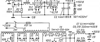
This is explained by the low efficiency of the first of these amplifiers, which creates certain difficulties associated with removing a significant amount of heat from the output transistors, as well as with the problem of ensuring the stability of the quiescent current. So, if in the final stage operating in AB mode, a change in this current by one and a half to two times is quite acceptable (although undesirable), then the same change in the quiescent current of amplifiers operating in mode A can lead to the most serious consequences. Modern powerful complementary transistors with a power dissipated at the collector of 100 watts or more mitigate this disadvantage of mode A, but they still use it mainly in UMZCH with a relatively low output power. The diagram of one such UMZCH is shown in Fig. 8. [16]. Main technical characteristics of the amplifier
| Rated input voltage, V | 1 |
| Rated output power, W | 12,5 |
| Load resistance. Ohm | 8 |
| Nominal frequency range (level - 3 dB), Hz | 5—225000 |
| Harmonic coefficient, %, in the frequency range 5 ... 20000 Hz with an output power of up to 10 W | 0,02 |
| Output voltage slew rate, V/µs | 10 |
| Relative background level, dB | -85 |
| Relative noise level, dB | -103 |
The peculiarity of this UMZCH is the use of both a transistor (VT1 and VT2) and an integrated op-amp (DA1 and DA2) in each of its arms. Both arms of the amplifier are covered by OOS. To reduce distortion, the gains of both arms must be the same, which is done subject to equality: R2/R1=R3/R4.
The quiescent current is stabilized by a tracking device consisting of a differential amplifier DA4 and an inverting voltage follower DA3. It works like this. Any fluctuation in the current flowing through the output transistors changes the voltage drop across resistors R22, R23, which is amplified by op-amp DA4 and supplied to the input of op-amp DA2, and
through inverter DA3 - to the input of op amp DA1. Circuits R19C3 and R20C11 form low-pass filters that pass only the lowest-frequency oscillations of the quiescent current to the output of op-amp DA4. The initial value of this current is set by resistor R26. Correction circuits R14C9 and R15C10 protect the amplifier from self-excitation. All op-amps are powered by a stabilized voltage of ± 18 V (the power circuits are not shown in the diagram). When repeating the amplifier, transistors MJ1001 and MJ901 can be replaced with KT827 with indices A, B and KT825 with indices G, D, respectively, the LM301 microcircuits can be replaced with op-amp K153UD2 (c metal case) or K553UD2 (in plastic). It is also possible to use op amps K157UD2 and K153UD6 (modification of op amp K153UD2) and other op amps with appropriate correction circuits and supply voltages (if they are below ±18 V, then, naturally, the output power of the amplifier will decrease).
Recently, it has been possible to significantly increase the efficiency of UMZCHs operating in mode A and bring it closer to the value characteristic of amplifiers operating in mode AB. This became possible thanks to the use of the output stage operating mode with a floating operating point (its position on the operating characteristic changes depending on the input signal level). In Fig. Figure 9 shows a schematic diagram of the output stage of the UMZCH [11], operating in this mode. As the voltage at the input of the amplifier increases, the current flowing through the load increases, and therefore through resistors R10 (positive half-wave), R11 (negative half-wave). As the voltage drop across these resistors increases, the current through resistors R7, R6 increases and, as a consequence, the base currents of transistors VT3, VT2 decrease and the voltages between their collectors and emitters increase. The latter circumstance leads to an increase in the bias voltage and a corresponding shift in the operating point of the output transistors to the region of higher quiescent current values.
In all stages of the amplifier, except for the final one (VT12 - VT15), you can use almost any low-power high-frequency transistors. To implement cascades on transistors VT4 - VT7 (“current mirrors”), transistor assemblies K159NT1V and KTS3103A are especially convenient. Complementary pairs of transistors KT814 and KT815, KT816 and KT817, KT818 and KT819 with any but identical letter indices can operate in the final stage.
Frequency correction of UMZCH. Reducing dynamic distortion can be achieved only by paying serious attention to the frequency correction of the UMZCH, covered by deep OOS. To better understand the issues related to the implementation of optimal frequency correction, consider the frequency response of a typical UMZCH with a transmission coefficient with an open circuit of the feedback equal to 60 dB, and with a closed circuit 26 dB (Fig. 10). To ensure such deep feedback throughout the entire audio frequency range, the amplifier's open-circuit feedback bandwidth must be no narrower than 20 kHz (the first bend in the frequency response at frequency f1). Next, the gain begins to decline with a slope of 20 dB per decade. The bandwidth of an amplifier with a closed feedback loop (frequency f2) is determined by the point of intersection of the frequency response of the UMZCH with a closed and open feedback loop and in our case is equal to 1 MHz. To prevent self-excitation of the amplifier, the frequency of the second inflection of the frequency response f3, which is determined, as a rule, by the cutoff frequency of the transistors of the final stage, should be in the region where the gain of the amplifier with open-loop feedback is less than 26 dB.
A real audio signal is pulsed in nature, so a good idea of the dynamic properties of an amplifier can be obtained from its response to a jump in input voltage. This reaction depends, as is known, on the transient response of the amplifier, which for UMZCH with the frequency response form discussed above can be described using the attenuation coefficient ξ calculated by the formula: ξ=1/2√f3/f2. The transient characteristics of the UMZCH for various values of this coefficient are shown in Fig. 11. By the magnitude of the first surge in the output voltage Uout=f(t), one can judge the relative stability of the amplifier. As can be seen from the figures shown. 11 characteristics, it is greatest at low attenuation coefficients. Such amplifiers are prone to self-excitation and, other things being equal, have high dynamic distortion. From the point of view of minimizing distortion, the best amplifier is with an aperiodic transient response (ξ>1). However, ensuring such a coefficient is achieved at too high a price. The fact is that in this case the amplifier must have an frequency response, the frequency of the second inflection f3 of which lies far beyond the bandwidth of the entire UMZCH with a closed circuit OOS (f3≥4f2). It is technically very difficult to implement such an amplifier, so you have to make a compromise by setting a lower attenuation coefficient. In the literature [9], the optimal attenuation coefficient is ξ=0.8, at which f3≥2.6f2, and the first surge of the output voltage does not exceed 1.4%.
The above relations are valid only for the linear region of the frequency response of the UMZCH, provided that the rate of rise of the amplifier's output voltage does not limit the duration of the transient process, and the frequency f3 sufficiently exceeds f2. If these conditions are not met, the transition process will be delayed and have a more pronounced oscillatory nature. If the frequency response of the UMZCH with an open circuit OOS is such that the gain Ku at frequency f2 is greater than 26 dB (dashed-dotted line in Fig. 10), then it is necessary to correct it to the required form. In two-stage UMZCHs, correction is most often carried out in the second stage, taking measures to ensure the required slew rate at the maximum output signal. It should be borne in mind that the maximum slew rate is not directly related to the small-signal bandwidth of the amplifier.
To set up the amplifier, rectangular pulses are applied to its input and, observing the transient process of the UMZCH on the oscilloscope screen, selecting a correction capacitor (C1 in Fig. 1 or Fig. 5) achieves a barely noticeable surge in the output voltage.
Thus, an UMZCH with low dynamic distortions must provide a transient process with ξ of at least 0.8 (see Fig. 11) and have a sufficient rate of rise of the output voltage. It is also necessary to fulfill the requirements for the linearization of all its cascades.
Some issues in the design of UMZCH. When designing high-quality UMZCHs, special attention should be paid to increasing its noise immunity. In order to avoid interference and the penetration of interference through the power circuits, it is necessary to carefully consider the installation, paying attention to the relative position of the conductors connecting the UMZCH with the signal source and the power supply, shield the installation areas sensitive to interference, provide good filtering of the supply voltage, etc. If the output stage operates in AB mode, then all components of the harmonic current, with the exception of the main one, circulate through the power wires. The parasitic inductive coupling between the power wires and the input circuits of the amplifier in poorly designed UMZCH leads to the fact that a parasitic EMF is induced in the input conductors, the frequency spectrum of which consists of harmonics of the amplified signal. For example, in an amplifier with an output power of 50 W at a load of 8 Ohms, operating from a correction amplifier for an electromagnetic pickup head with an output voltage of 1 mV, additional distortion (at the second harmonic of the signal) amounted to approximately 0.33% for each nH of parasitic coupling inductance [15 ]. To eliminate this undesirable effect, it is necessary to separate the power wires and signal circuits of the UMZCH. It is even better to include additional filtering RC circuits in the supply circuits (for example, R5C1 and R6C2 in the amplifier according to the diagram in Fig. 12), placing them directly on the UMZCH circuit board.
The finite resistance of the “ground” buses leads to the fact that current pulses through the common wire from the output of the UMZCH can reach its input. To combat such interference, it is usually recommended to increase the cross-section of the common wire buses and connect all the conductors going to them at one point. But the most effective method of protection is galvanic isolation of the common wire of the input stage from the powerful power bus. This is possible in an UMZCH with a differential input stage. Only the terminals of resistors R1 and R2 are connected to the common wire of the signal source (the left one in the diagram in Fig. 12). All other conductors connected to the common wire are connected to a powerful power supply bus (on the right in the diagram). However, in this case, turning off the signal source for any reason can lead to failure of the UMZCH, since the left “ground” bus is not connected to anything and the state of the output stage becomes unpredictable. To avoid this situation, both “ground” buses are connected by resistor R4. Its resistance should not be very small so that interference from a powerful power bus cannot penetrate the amplifier input, and at the same time not too large so as not to affect the depth of the feedback. In practice, the resistance of the protective resistor is chosen in the range from units to tens of ohms.
Ways to improve UMZCH. In recent years, there has been a tendency to improve the quality indicators of UMZCH by building completely push-pull (including input stages) amplifiers with powerful MOS transistors (with an insulated gate) in the output stage. Compared to bipolar MOS transistors, they are favorably distinguished by better linearity of pass-through characteristics, high input impedance, and good frequency properties. They do not have the phenomenon of secondary thermal breakdown, since with increasing crystal temperature, due to high power dissipation, the resistance of the transistor channel increases. This allows in some cases to do without protecting the UMZCH from thermal overloads. As an example in Fig. Figure 13 shows a diagram of a fully push-pull amplifier with complementary pairs of powerful MOS transistors in the Japanese output stage [12].
Main technical characteristics
| Rated output power, W | 120 | |
| Load resistance, Ohm | 8 | |
| Gain, dB | 26 | |
| Harmonic distortion, %, at rated output power at frequency: | ||
| 1,000 Hz | 0,002 | |
| 10,000 Hz | 0,0065 | |
| OOS depth, dB | 40 | |
| Maximum slew rate of output voltage (without input filter), V/µs | 60 | |
The push-pull input stage (VT1, VT2; VT4, VT6) made it possible to get by with simple current sources using transistors VT3 and VT5. The voltage amplifier is built according to a circuit similar to that shown in Fig. 6. To increase the output power, the final stage transistors VT14, VT16 (2SKI34) and VT15, VT17 (2SJ49) are connected in parallel. Filter R1C2 protects the UMZCH input from high-frequency interference. To avoid imbalance of the amplifiers due to input currents, resistors R2 and R27 of the same resistance are connected to the non-inverting and inverting inputs.
In this amplifier, the common wires of the input and output stages are separated (see the previous section), as indicated by the image of resistor R23. Such an implicit indication of the separation of common buses is often found in UMZCH circuits published in foreign publications.
The limited volume of the journal article did not allow us to introduce readers to other interesting circuit solutions of the UMZCH, so we recommend that those interested in this topic refer to the literature listed in the attached list.
LITERATURE
- Cherry Edward M. Amplitude and Phase of Intermodulation Distortion.—Journal of the Audio Engineering Society, 1983, v. 31. No. 5, p. 298-303.
- Cordell Robert R. Another View on TIM. Part 1.—Audio. 1980, v. 64 No. 2, p. 38-49.
- Cordell Robert R. Phase Intermodulation Distortion Instrumentation and Measurements.— Journal of the Audio Engineering Society, 1983. v. 31. No. 3, p. 114-123.
- Krauter M. Nf-Verstarker: Der Gesamt-eindruck zait, - Funkschau, 1983, No. 18, 59-61.
- Petrl—Larml M., Otala M., Lammasmieml J. Psychoacoustic Detection Threshold of Transient Intermodulation Distortion.— Journal of the Audio Engineering Society, 1980. v. 28, no. 3, p. 98-104.
- Got it I. Operational amplifiers. Per. from English - M.: Mir, 1982.
- Scott Robert F. Power MOSFET Amplifiers.—Radio—Electronics. 1983.v. 54, no. 7, p. 80-81.
- Leach Marshall W. An Amplifier Input Stage Design Criterion for the Suppression of Dynamic Distortions.— Journal of the Audio Engineering Society, 1981. v. 29, No. 4. p. 249-251.
- Cherry Edward M. Transient Intermodulation Distortion. - Part I: Hard Nonlinearity. - IEEE Transactions on Acoustics, Speech, and Signal Processing, 1981. v. ASSP—29, no. 2. p. 137-146.
- Cherry Edward M. Feedback. Sensitivity, and Stability of Audio Power Amplifiers.—Journal of the Audio Engineering Society, 1982, v. 30, no. 5. p. 282-294.
- Kondo Hikaru. Nuevo conceplo en amplificadores de potencia para audio sistema “super A” de JVC.—Mundo eleutronico, 1980, no. 102, p. 75-81.
- Borbely Erno. High Power High Quality Amplifier Using MOSFETs.—Wireless World. 1983, v. 89. No. 1556. p. 69-75.
- Cordell Robert R. Another View of TIM. Part 2.—Audio. 1980, v. 64. No. 3. p. 39-40.
- Titze U., Schenk K. Semiconductor circuitry. Help Guide. Per. from German.— M.: Mir, 1982, p. 240.
- Pollock N. 12 W class A power amplifier.—Wireless World. 1980. Vol. 86. No. 1529, to. 74.
- Jung Walter G., Marsh Richard. Selection Capacitors for Optimum Performance. Part I.—Audio, 1980. Vol. 64. No. 2. p. 52-86.
- Cherry Edward M. A New Distortion Mechanism It Class B. Amplifiers.— journal of the Audio Engineering Society. 1981. Vol. 20, No. 5. p. 327-328.
- Efremov V.S. Push-pull amplifiers with stabilization of minimum shoulder currents.—Semiconductor electronics in communications technology.—M.: Radio and Communications, 1983. issue. 93, p. 87-94.
- Sandman A, Low cross-over distortion class B amplifier.— Wireless World. 1971. Vol. 77. No. 1429, p. 341.
- Horowitz Mannle. How to Design Analog Circuits. Audio Power Amplifiers.—Radio-Etectronics, 1983, Vol. 54. No. 5, p. 73-76.
- Hood Llnaley JL 60-100 W MOSFET Audio Amplifier.— Wireless World, 1982, Vol. 88. No. 1558, p. 83-86.
Radio No. 5,6 1985
Amplifier output power
The output power of the amplifier delivered to the active load will be expressed by the formula:
Where
Pout - amplifier output power, W
Iout - current strength in the load circuit, A
UOut—load voltage, V
The power to the load with a reactive component will already be expressed through the formula:
Where
Pout - amplifier output power, W
Iout - current strength in the load circuit, A
Uout—load voltage, V
cosφ - where φ is the phase difference between the current and voltage oscillogram
For example, the phase difference between current and voltage in a resistive load is zero, therefore cos0=1. Therefore, the formula for the active load takes the form
You can read more about this in the article about active and reactance.
The maximum output power at which the distortion of the output signal does not exceed the quality values of the amplifier is called the rated power of the amplifier .
Well, a general rule, in order to make it easier to remember all these three types of amplifier:
In UN KU > 1, KI = 1; in UT KI > 1, KU = 1; in the mind KU > 1 and KI > 1.
Class D
This type of device makes it possible to create your own modular systems. Using the equipment, high-quality processing of the entire outgoing stream is carried out. Designing audio power amplifiers allows you to create your own multimedia system for work or entertainment. However, there are some nuances here. Often erroneously referred to as digital amplification, Class D converters represent a guarantee of unit efficiency, achieving gains in excess of 90% in real-world testing.
The first question to address is why this is class D if "digital amplification" is a misnomer. It was simply the next letter in the alphabet, with Class C used in audio systems. More importantly, how can 90%+ efficiency be achieved. While all of the previously mentioned classes of amplifiers have one or more output devices that are constantly active, even when the converter is actually in standby mode, Class D units quickly switch them between "off" and "on". This is quite convenient and makes it possible to use the module only at the right moments.
For example, the design of class T audio amplifiers, which are an implementation of class D developed by Tripath, uses switching frequencies of about 50 MHz, unlike the basic device. Output devices are usually controlled by pulse width modulation. This is where square waves of varying widths are generated by a modulator that presents an analog signal for playback. By strictly controlling the output devices in this way, 100% efficiency is theoretically possible (though obviously not achievable in the real world).
Delving deeper into the world of Class D audio amplifiers, you can also find mention of analog and digital controllable modules. These control units have an analog input signal and an analog control system, usually with some degree of feedback error correction. On the other hand, digital conversion Class D amplifiers use digital control that switches the power stage without error control. This solution also meets with approval, according to reviews from many customers. However, the price segment here is much higher.
Audio amplifier research has shown that analog-driven Class D has a performance advantage over its digital counterpart, as it typically offers lower output impedance (resistance) and an improved distortion profile. This increases the initial values of the system at its maximum load.
The parameters of audio amplifiers are much higher than those of basic models. It is worth understanding that such calculations are required only for creating music in the studio. Regular buyers can skip these features.
This is usually an L network (inductor and capacitor) placed between the amplifier and speakers to reduce the noise associated with Class D operation. The filter is important. Poor design can compromise efficiency, reliability and sound quality. In addition, feedback after the output filter has its advantages. Although designs that do not use feedback at this stage can tune their response to a specific impedance, when such amplifiers have a complex load (that is, a loudspeaker rather than a resistor), the frequency response can vary significantly depending on the load on the speaker. Feedback stabilizes this problem, ensuring smooth response to complex loads.
Ultimately, the complexity of Class D electrical audio amplifiers has its benefits. Efficiency and, as a result, less weight. Since relatively little energy is spent on heat, much less energy is required. Thus, many Class D amplifiers are used in combination with switching mode power supplies (SMPS). Like the output stage, the power supply itself can be quickly turned on and off to regulate voltage, resulting in further improvements in efficiency and the ability to reduce weight relative to traditional analog/linear power supplies.
Taken together, even powerful Class D amplifiers can weigh only a few kilograms. The disadvantage of SMPS power supplies compared to traditional linear supplies is that the former usually do not have much dynamic headroom.
Trials and extensive testing of Class D audio amplifiers with linear power supplies versus SMPS modules have shown that this is indeed the case. When two amplifiers handled rated power, but one with a linear power supply could produce higher dynamic power levels. However, SMPS designs are becoming more common and you can expect to see higher quality, next generation Class D units using similar shapes in stores.
Types of amplifiers by bandwidth
Based on bandwidth, amplifiers are divided into:
Low Frequency Amplifiers
They are also called audio frequency amplifiers (AF). They are designed to amplify signals with frequencies from tens of Hertz to 20 kHz. 20 kHz is the limit of frequency that can be perceived by the human ear. Therefore, this type of amplifier is very popular among music lovers and radio amateurs.
High frequency amplifiers
They are designed to amplify signals over the entire range of frequencies used by electronics.
Broadband amplifiers
They allow amplification of a wide frequency band (for example, from tens of hertz to several megahertz). Here, I think, everything is clear.
Narrowband amplifiers
They amplify a narrow frequency band. These can be resonant filters, as well as filters that are based on UHF and ULF.
Class division
If users have ever looked at an audio power amplifier datasheet, they may have noticed equipment classes usually designated by a letter or two. The most common block types used in consumer home audio today are A, A/B, D, G, and H values.
These classes are not simple classification systems, but descriptions of amplifier topology, that is, how they function at the core level. While each type of amplifier has its own set of strengths and weaknesses, their performance (and how the final performance is judged) remains the same.
It consists of converting the waveform sent by the pre-unit without introducing interference, or at least as little distortion as possible.